ZHCSKW8C February   2020  – September 2023 ADS7066

PRODUCTION DATA  

  1.   1
  2. 特性
  3. 应用
  4. 说明
  5. Revision History
  6. Pin Configuration and Functions
  7. Specifications
    1. 6.1 Absolute Maximum Ratings
    2. 6.2 ESD Ratings
    3. 6.3 Recommended Operating Conditions
    4. 6.4 Thermal Information
    5. 6.5 Electrical Characteristics
    6. 6.6 Timing Requirements
    7. 6.7 Switching Characteristics
    8. 6.8 Timing Diagrams
    9. 6.9 Typical Characteristics
  8. Detailed Description
    1. 7.1 Overview
    2. 7.2 Functional Block Diagram
    3. 7.3 Feature Description
      1. 7.3.1  Analog Input and Multiplexer
      2. 7.3.2  Reference
        1. 7.3.2.1 External Reference
        2. 7.3.2.2 Internal Reference
      3. 7.3.3  ADC Transfer Function
      4. 7.3.4  ADC Offset Calibration
      5. 7.3.5  Programmable Averaging Filters
      6. 7.3.6  CRC on Data Interface
      7. 7.3.7  Oscillator and Timing Control
      8. 7.3.8  Diagnostic Modes
        1. 7.3.8.1 Bit-Walk Test Mode
        2. 7.3.8.2 Fixed Voltage Test Mode
      9. 7.3.9  Output Data Format
        1. 7.3.9.1 Status Flags
        2. 7.3.9.2 Output CRC (Device to Host)
        3. 7.3.9.3 Input CRC (Host to Device)
      10. 7.3.10 Device Programming
        1. 7.3.10.1 Enhanced-SPI Interface
        2. 7.3.10.2 Daisy-Chain Mode
        3. 7.3.10.3 Register Read/Write Operation
          1. 7.3.10.3.1 Register Write
          2. 7.3.10.3.2 Register Read
            1. 7.3.10.3.2.1 Register Read With CRC
    4. 7.4 Device Functional Modes
      1. 7.4.1 Device Power-Up and Reset
      2. 7.4.2 Manual Mode
      3. 7.4.3 On-the-Fly Mode
      4. 7.4.4 Auto-Sequence Mode
    5. 7.5 ADS7066 Registers
  9. Application and Implementation
    1. 8.1 Application Information
    2. 8.2 Typical Application
      1. 8.2.1 Design Requirements
      2. 8.2.2 Detailed Design Procedure
        1. 8.2.2.1 Charge-Kickback Filter and ADC Amplifier
      3. 8.2.3 Application Curve
    3. 8.3 Power Supply Recommendations
      1. 8.3.1 AVDD and DVDD Supply Recommendations
    4. 8.4 Layout
      1. 8.4.1 Layout Guidelines
      2. 8.4.2 Layout Example
  10. Device and Documentation Support
    1. 9.1 Device Support
      1. 9.1.1 Development Support
    2. 9.2 Documentation Support
      1. 9.2.1 Related Documentation
    3. 9.3 接收文档更新通知
    4. 9.4 支持资源
    5. 9.5 Trademarks
    6. 9.6 静电放电警告
    7. 9.7 术语表
  11. 10Mechanical, Packaging, and Orderable Information

封装选项

机械数据 (封装 | 引脚)
散热焊盘机械数据 (封装 | 引脚)
订购信息

ADC Transfer Function

The ADC output is in straight binary format. The full-scale input range (FSR) of the ADC is determined by the RANGE bit. On power-up, the FSR is 0 V to VREF. When using the 2 x VREF mode (RANGE = 1b), the ADC can measure analog inputs up to two times the voltage reference. Equation 1 can be used to compute the ADC resolution:


Equation 1. 1 LSB = FSR / 2N

where:

  • FSR = Full-scale input range of the ADC
  • N = 16

Figure 7-2 and Table 7-1 show the ideal transfer characteristics for this device.
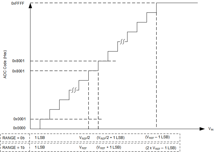
GUID-34B7B020-8FB3-49B0-B6C7-9C408386B955-low.gifFigure 7-2 Ideal Transfer Characteristics
Table 7-1 Transfer Characteristics
INPUT VOLTAGE CODE IDEAL OUTPUT CODE
RANGE = 0b RANGE = 1b
≤1 LSB ≤1 LSB Zero 0000
1 LSB to 2 LSBs 1 LSB to 2 LSBs Zero + 1 0001
(VREF / 2) to (VREF / 2) + 1 LSB VREF to VREF + 1 LSB Mid-scale code 8000
(VREF / 2) + 1 LSB to (VREF / 2) + 2 LSBs VREF + 1 LSB to VREF + 2 LSBs Mid-scale code + 1 8001
≥ VREF – 1 LSB ≥ 2 x VREF – 1 LSB Full-scale code FFFF