SLAS669E September 2010 – may 2020 ADS5400-SP
PRODUCTION DATA.
- 1 Features
- 2 Applications
- 3 Description
- 4 Revision History
- 5 Pin Configuration and Functions
- 6 Specifications
-
7 Detailed Description
- 7.1 Overview
- 7.2 Functional Block Diagram
- 7.3 Feature Description
- 7.4 Device Functional Modes
- 7.5 Programming
- 7.6 Serial Register Map
- 8 Application and Implementation
- 9 Power Supply Recommendations
- 10Layout
- 11Device and Documentation Support
- 12Mechanical, Packaging, and Orderable Information
8.2 Typical Application
The analog inputs of the ADS5400-SP must be fully differential and biased to an appropriate common mode voltage, VCM. It is rare that the end equipment has a signal that already meets the requisite amplitude and common mode and is fully differential. Therefore, there is a signal conditioning circuit for the analog input. If the amplitude of the input circuit is such that no gain is needed to make full use of the full-scale range of the ADC, then a transformer coupled circuit as used on the EVM may be used with good results. The transformer coupling is inherently low-noise, and inherently AC-coupled so that the signal may be biased to VCM after the transformer coupling.
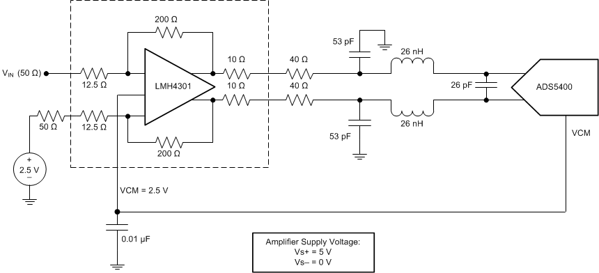
If signal gain is required, or the input bandwidth is to include the spectrum all the way down to DC such that AC coupling is not possible, then an amplifier-based signal conditioning circuit would be required. shows LMH3401 interfaced with ADS5400-SP. LMH3401 is configured to have to Single-Ended input with a differential outputs follow by 1st Nyquist based low pass filter with 400 MHz bandwidth. Figure 38 also shows the power supply recommendations for the amplifier.
 Figure 38. ADS5400-SP Input Circuit Using an LMH3401 Fully Differential Amplifier
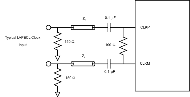
 Clocking a High Speed ADC such as the ADS5400-SP requires a fully differential clock signal from a clean, low-jitter clock source and driven by an appropriate clock buffer, often with LVPECL or LVDS signaling levels. The sample clock must be biased up to the appropriate common-mode voltage, and the device will internally bias the clock to the appropriate common-mode voltage if the clock signal is AC-coupled as shown in Figure 39.
 Figure 39. Recommended Differential Clock Driving Circuit