ZHCSE48B September 2015 – January 2019 ADC31JB68
PRODUCTION DATA.
- 1 特性
- 2 应用
- 3 说明
- 4 修订历史记录
- 5 Pin Configuration and Functions
- 6 Specifications
- 7 Parameter Measurement Information
-
8 Detailed Description
- 8.1 Overview
- 8.2 Functional Block Diagram
- 8.3
Feature Description
- 8.3.1 Analog Inputs and Input Buffer
- 8.3.2 Amplitude and Phase Imbalance Correction
- 8.3.3 Over-Range Detection
- 8.3.4 Input Clock Divider
- 8.3.5 SYSREF Detection Gate
- 8.3.6 Serial Differential Output Drivers
- 8.3.7 ADC Core Calibration
- 8.3.8 Data Format
- 8.3.9 JESD204B Supported Features
- 8.3.10 JESD204B Interface
- 8.3.11 Transport Layer Configuration
- 8.3.12 Test Pattern Sequences
- 8.3.13 JESD204B Link Initialization
- 8.3.14 SPI
- 8.4 Device Functional Modes
- 8.5
Register Map
- 8.5.1
Register Descriptions
- 8.5.1.1 CONFIG_A (address = 0x0000) [reset = 0x3C]
- 8.5.1.2 DEVICE CONFIG (address = 0x0002) [reset = 0x00]
- 8.5.1.3 CHIP_TYPE (address = 0x0003 ) [reset = 0x03]
- 8.5.1.4 CHIP_ID (address = 0x0005, 0x0004) [reset = 0x00, 0x1B]
- 8.5.1.5 CHIP_VERSION (address =0x0006) [reset = 0x00]
- 8.5.1.6 VENDOR_ID (address = 0x000D, 0x000C) [reset = 0x04, 0x51]
- 8.5.1.7 SPI_CFG (address = 0x0010 ) [reset = 0x01]
- 8.5.1.8 OM1 (Operational Mode 1) (address = 0x0012) [reset = 0xC1]
- 8.5.1.9 OM2 (Operational Mode 2) (address = 0x0013) [reset = 0x20]
- 8.5.1.10 IMB_ADJ (Imbalance Adjust) (address = 0x0014) [reset = 0x00]
- 8.5.1.11 OVR_EN (Over-Range Enable) (address = 0x003A) [reset = 0x00]
- 8.5.1.12 OVR_HOLD (Over-Range Hold) (address = 0x003B) [reset = 0x00]
- 8.5.1.13 OVR_TH (Over-Range Threshold) (address = 0x003C) [reset = 0x00]
- 8.5.1.14 DC_MODE (DC Offset Correction Mode) (address = 0x003D) [reset = 0x00]
- 8.5.1.15 SER_CFG (Serial Lane Transmitter Configuration) (address = 0x0047) [reset = 0x00]
- 8.5.1.16 JESD_CTRL1 (JESD Configuration Control 1) (address = 0x0060) [reset = 0x7F]
- 8.5.1.17 JESD_CTRL2 (JESD Configuration Control 2) (address = 0x0061) [reset = 0x00]
- 8.5.1.18 JESD_RSTEP (JESD Ramp Pattern Step) (address = 0x0063, 0x0062) [reset = 0x00, 0x01]
- 8.5.1.19 SER_INV (Serial Lane Inversion Control) (address = 0x0064) [reset = 0x00]
- 8.5.1.20 JESD_STATUS (JESD Link Status) (address = 0x006C) [reset = N/A]
- 8.5.1
Register Descriptions
- 9 Application and Implementation
- 10Power Supply Recommendations
- 11Layout
- 12器件和文档支持
- 13机械、封装和可订购信息
6.8 Timing Requirements
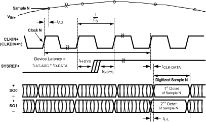
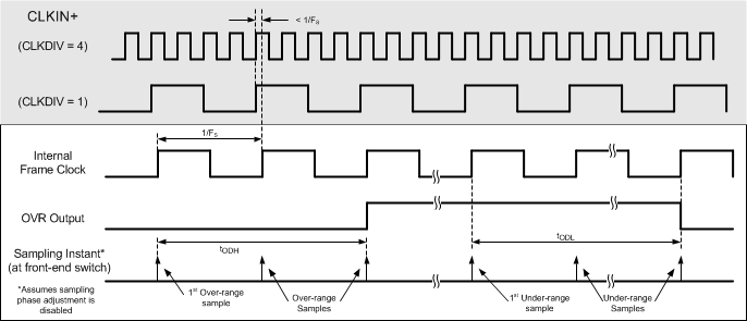
typical values at TA = 25°C, full temperature range is TMIN = –40°C to TMAX = 85°C, ADC sampling rate = 500 MSPS, 50% clock duty cycle, VA3.0 = 3 V; VA1.8 = 1.8 V; VA1.2 = VACLK1.2 = 1.2 V; –1 dBFS differential input, and R(term) = 100 Ω (unless otherwise noted) (see Figure 1 and Figure 2 for timing diagrams)| PARAMETER | NOTES | MIN | NOM | MAX | UNIT | |
|---|---|---|---|---|---|---|
| ADC SAMPLING INSTANT TIMING CHARACTERISTICS | ||||||
| FS | Sampling rate | Equal to FCLKIN / CLKDIV | 100 | 500 | MSPS | |
| FCLKIN | Input clock frequency at CLKIN inputs | CLKDIV = 1 | 100 | 500 | MHz | |
| CLKDIV = 2 | 200 | 1000 | ||||
| CLKDIV = 4 | 400 | 2000 | ||||
| DC | Input clock (CLKIN) duty cycle | CLKDIV = 1 | 50% ± 20% | |||
| CLKDIV = 2 or CLKDIV = 4 | 50% ± 5% | |||||
| tLAT-ADC | ADC core latency | Delay from a reference sampling instant to the boundary of the internal LMFC where the reference sample is the first sample of the next transmitted multi-frame. In this device, the frame clock period is equal to the sampling clock period. | 7 | Frame clock cycles | ||
| tJ | Additive sampling aperture jitter | Depends on input CLKIN differential edge rate at the zero crossing, dVSS/dt, tested with 5 V/ns edge rate. | fs | |||
| CLKDIV = 1 | 80 | |||||
| CLKDIV = 2, 4 | 90 | |||||
| OVER-RANGE INTERFACE TIMING CHARACTERISTICS (SDO/OVR(1)) | ||||||
| tODH | OVR assertion delay | Functional delay between an overrange value sampled and OVR asserted | 8 | Frame clock cycles | ||
| tODL | OVR de-assertion delay | Functional delay between first underrange value sampled until OVR de-assertion, configurable via SPI | Frame clock cycles | |||
| Configured for minimum delay | tODH | |||||
| Configured for maximum delay | tODH + 15 | |||||
| SYSREF TIMING CHARACTERISTICS | ||||||
| tPH-SYS | SYSREF assertion duration | Required duration of SYSREF assertion after rising edge event | 2 | Frame clock cycles | ||
| tPL-SYS | SYSREF de-assertion duration | Required duration of SYSREF de-assertion after falling edge event | 2 | Frame clock cycles | ||
| tS-SYS | SYSREF setup time | Relative to CLKIN rising edge | 350 | ps | ||
| tH-SYS | SYSREF hold time | Relative to CLKIN rising edge | 0 | ps | ||
| JESD204B INTERFACE LINK TIMING CHARACTERISTICS | ||||||
| tD-LMFC | SYSREF to LMFC delay | Functional delay between SYSREF assertion latched and LMFC frame boundary. Depends on CLKDIV setting | ||||
| CLKDIV = 1 | 4 | CLKIN cycles | ||||
| 4 | Frame clock cycles | |||||
| CLKDIV = 2 | 10 | CLKIN cycles | ||||
| 5 | Frame clock cycles | |||||
| CLKDIV = 4 | 18 | CLKIN cycles | ||||
| 4.5 | Frame clock cycles | |||||
| tD-K28 | LMFC to K28.5 delay | Functional delay between the start of the first K28.5 frame during code group synchronization at the serial output and the preceding LMFC frame boundary | 5.6 | 6.6 | 7.6 | Frame clock cycles |
| tD-ILA | LMFC to ILA delay | Functional delay between the start of the first ILA frame during initial lane synchronization at the serial output and the preceding LMFC frame boundary | 5.6 | 6.6 | 7.6 | |
| tD-DATA | LMFC to valid data delay | Functional delay between the start of the first valid data frame at the serial output and the preceding LMFC frame boundary | 5.6 | 6.6 | 7.6 | |
| tS-SYNCb-F | SYNCb setup time | Required SYNCb setup time-relative to the internal LMFC boundary(2) | 3 | Frame clock cycles | ||
| tH-SYNCb-F | SYNCb hold time | Required SYNCb hold time relative to the internal LMFC boundary(2) | 0 | |||
| tH-SYNCb | SYNCb assertion hold time | Required SYNCb hold time after assertion before de-assertion to initiate a link resynchronization | 4 | |||
| tILA | ILA duration | Duration of the ILA sequence | 4 | Multi-frame
clock cycles |
||
| SERIAL OUTPUT DATA TIMING CHARACTERISTICS | ||||||
| FSR | Serial bit rate | 1 | 5.0 | Gb/s | ||
| UI | Unit interval | 5.0 Gb/s data rate | 200 | ps | ||
| tR, tF | Rise/fall times | 5.0 Gb/s data rate, default values for VOD and DEM | 43 | ps | ||
| DJ | Deterministic jitter | Includes periodic jitter (PJ), data dependent jitter (DDJ), duty cycle distortion (DCD), and inter-symbol interference (ISI); 5.0 Gb/s data rate | 0.049 | p-p UI | ||
| 9.82 | p-p ps | |||||
| RJ | Random jitter | Assumes BER of 1e-15 (Q = 15.88); 5.0 Gb/s data rate | 0.119 | p-p UI | ||
| 1.50 | rms ps | |||||
| TJ | Total jitter | Sum of DJ and RJ, assumes BER of 1e-15 (Q = 15.88); 5.0 Gb/s data rate | 0.169 | p-p UI | ||
| 33.6 | p-p ps | |||||
| SPI BUS TIMING CHARACTERISTICS(3) | ||||||
| ƒSCLK | Serial clock frequency | fSCLK = 1 / tP | 20 | MHz | ||
| tPH | SCLK pulse width – high | 6 | ns | |||
| tPL | SCLK pulse width – low | 7 | ns | |||
| tSSU | SDI input data setup time | 3 | ns | |||
| tSH | SDI input data hold time | 1 | ns | |||
| tODZ | SDO output data driven-to-3-state time | 10 | ns | |||
| tOZD | SDO output data 3-state-to-driven time | 25 | ns | |||
| tOD | SDO output data delay time | 25 | ns | |||
| tCSS | CSB setup time | 3 | ns | |||
| tCSH | CSB hold time | 1 | ns | |||
| tIAG | Inter-access gap | Minimum time CSB must be de-asserted between accesses | 1 | ns | ||
(1) The SDO/OVR pin is configured in over-range output mode.
(2) The SYNCb setup and hold times determine the multi-frame after which the ILA is initiated but meeting the setup and hold times are not required to achieve deterministic latency.
(3) All timing specifications for the SPI given for VSPI = 1.8-V logic levels and a 5-pF capacitive load on the SDO pin. Timing specification require larger margins for VSPI= 1.2 V. The serial bit rate of the SPI should be limited to 10 Mb/s or lower for VSPI = 1.2-V logic.
 Figure 1. Sample Timing Diagram
  Figure 2. Overrange (OVR) Timing Diagram
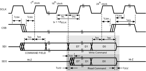
  Figure 3. SPI Timing Diagram