ZHCSEE8B December 2015 – April 2017 ADC14X250
PRODUCTION DATA.
- 1 特性
- 2 应用范围
- 3 说明
- 4 修订历史记录
- 5 Pin Configuration and Functions
-
6 Specifications
- 6.1 Absolute Maximum Ratings
- 6.2 ESD Ratings
- 6.3 Recommended Operating Conditions
- 6.4 Thermal Information
- 6.5 Electrical Characteristics: Static Converter Performance
- 6.6 Electrical Characteristics: Dynamic Converter Performance
- 6.7 Electrical Characteristics: Power Supply
- 6.8 Electrical Characteristics: Analog Interface
- 6.9 Digital Input Characteristics
- 6.10 Electrical Characteristics: Serial Data Output Interface
- 6.11 Electrical Characteristics: Digital Input
- 6.12 Timing Requirements
- 6.13 Typical Characteristics
- 7 Parameter Measurement Information
-
8 Detailed Description
- 8.1 Overview
- 8.2 Functional Block Diagram
- 8.3
Feature Description
- 8.3.1 Amplitude and Phase Imbalance Correction of Differential Analog Input
- 8.3.2 Input Clock Divider
- 8.3.3 SYSREF Offset Feature and Detection Gate
- 8.3.4 DC Offset Correction
- 8.3.5 Serial Differential Output Drivers
- 8.3.6 ADC Core Calibration
- 8.3.7 Data Format
- 8.3.8 JESD204B Supported Features
- 8.3.9 Transport Layer Configuration
- 8.3.10 Test Pattern Sequences
- 8.3.11 JESD204B Link Initialization
- 8.3.12 Sync~ Signal Selection
- 8.3.13 SPI
- 8.4 Device Functional Modes
- 8.5
Register Map
- 8.5.1
Register Descriptions
- 8.5.1.1 CONFIG_A, [Address: 0x0000], [Default: 0x3C]
- 8.5.1.2 DEVICE CONFIG, [Address: 0x0002], [Default: 0x00]
- 8.5.1.3 CHIP_TYPE, [Address: 0x0003], [Default: 0x03]
- 8.5.1.4 CHIP_ID, [Address: 0x0005, 0x0004], [Default: 0x00, 0x01]
- 8.5.1.5 CHIP_VERSION, [Address: 0x0006], [Default: 0x00]
- 8.5.1.6 VENDOR_ID, [Address: 0x000D, 0x000C], [Default: 0x04, 0x51]
- 8.5.1.7 SPI_CFG, [Address: 0x0010], [Default: 0x01]
- 8.5.1.8 OM1 (Operational Mode 1), [Address: 0x0012], [Default: 0x81]
- 8.5.1.9 OM2 (Operational Mode 2), [Address: 0x0013], [Default: 0x20]
- 8.5.1.10 IMB_ADJ (Imbalance Adjust), [Address: 0x0014], [Default: 0x00]
- 8.5.1.11 DC_MODE (DC Offset Correction Mode), [Address: 0x003D], [Default: 0x00]
- 8.5.1.12 SER_CFG (Serial Lane Transmitter Configuration), [Address: 0x0047], [Default: 0x00]
- 8.5.1.13 JESD_CTRL1 (JESD Configuration Control 1) , [Address: 0x0060], [Default: 0x7D]
- 8.5.1.14 JESD_CTRL2 (JESD Configuration Control 2), [Address: 0x0061], [Default: 0x00]
- 8.5.1.15 JESD_RSTEP (JESD Ramp Pattern Step), [Addresses: 0x0063, 0x0062], [Default: 0x00, 0x01]
- 8.5.1.16 JESD_STATUS (JESD Link Status), [Address: 0x006C], [Default: N/A]
- 8.5.1
Register Descriptions
- 9 Application and Implementation
- 10Power Supply Recommendations
- 11Layout
- 12器件和文档支持
- 13机械、封装和可订购信息
5 Pin Configuration and Functions
RHB package
32 Pin WQFN
Top View
Exposed pad on bottom of package
Pin Functions
| PIN | TYPE OR DIAGRAM | DESCRIPTION | |
|---|---|---|---|
| NAME | NO. | ||
| AGND | 2, 5, 8, 11, 18, 21, 27, 30, 31 | Analog ground | Analog ground Must be connected to a solid ground reference plane under the device. |
| BP2.5 | 22 | Bypass pins | Capacitive bypassing pin for internally regulated 2.5-V supply This pin must be decoupled to AGND with a 0.1-μF and a 10-µF capacitor located close to the pin. |
| CLKIN+ | 9 |
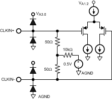 |
Differential device clock input pins Each pin is internally terminated to a DC bias with a 50-Ω resistor for a 100-Ω total internal differential termination. AC coupling is required for coupling the clock input to these pins if the clock driver cannot meet the common-mode requirements. Sampling occurs on the rising edge of the differential signal (CLKIN+) − (CLKIN–). |
| CLKIN– | 10 | ||
| CSB | 23 |
 |
SPI chip select pin When this signal is asserted, SCLK is used to clock the input serial data on the SDI pin or output serial data on the SDO pin. When this signal is de-asserted, the SDO pin is high impedance and the input data is ignored. Active low. A 10 kΩ pull-up resistor to a supply corresponding to the CSB drive logic level is recommended to prevent undesired activation of the SPI bus. Compatible with 1.2- to 3-V CMOS logic levels. |
| SO+ | 19 |
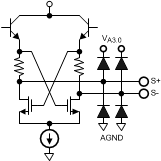 |
Differential high speed serial data lane pins These pins must be AC coupled to the receiving device. The differential trace routing from these pins must maintain a 100-Ω characteristic impedance. |
| SO– | 20 | ||
| SCLK | 24 |
 |
SPI serial clock pin Serial data is shifted into and out of the device synchronous with this clock signal. Compatible with 1.2- to 3-V CMOS logic levels. |
| SDI | 25 | SPI data input pin Serial data is shifted into the device on this pin while the CSB signal is asserted. Compatible with 1.2- to 3-V CMOS logic levels. |
|
| SDO | 26 |
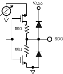 |
SPI data output pin Serial data is shifted out of the device on this pin during a read command while CSB is asserted. The output logic level is configurable as 1.2, 1.8, 2.5, or 3 V. The output level must be configured after power up and before performing a read command. See the Register Descriptions for configuration details. |
| SYNCb+ | 15 |
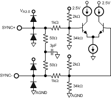 |
Differential SYNCb signal input pins DC coupling is required for coupling the SYNCb signal to these pins. Each pin is internally terminated to the DC bias with a large resistor. An internal 100-Ω differential termination is provided therefore an external termination is not required. Additional resistive components in the input structure give the SYNCb input a wide input common-mode range. The SYNCb signal is active low and therefore asserted when the voltage at SYNCb+ is less than at SYNCb–. If JESD204B sync~ signals are directed via SPI (with SYNC_SEL=1), then SYNCb+ and SYNCb- may remain not connected. |
| SYNCb– | 16 | ||
| SYSREF+ | 13 |
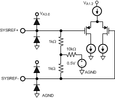 |
Differential SYSREF signal input pins Each pin is internally terminated to a DC bias with a 1-kΩ resistor. An external 100-Ω differential termination must always be provided. AC coupling using capacitors is required for coupling the SYSREF signal to these pins if the clock driver cannot meet the common-mode requirements. In the case of AC coupling, the external termination must be placed on the source side of the coupling capacitors. |
| SYSREF– | 14 | ||
| VA1.2 | 7, 17, 28 | Supply input pin | 1.2-V analog power supply pins These pins must be connected to a quiet source and decoupled to AGND with a 0.1-μF and 0.01-μF capacitor located close to each pin. |
| VA1.8 | 12, 29, 32 | Supply input pin | 1.8-V analog power supply pins These pins must be connected to a quiet source and decoupled to AGND with a 0.1-μF and 0.01-μF capacitor located close to each pin. |
| VA3.0 | 1 | Supply input pin | 3-V analog power supply pin This pin must be connected to a quiet source and decoupled to AGND with a 0.1-μF and 0.01-μF capacitor located close to the pin. |
| VCM | 6 |
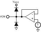 |
Input interface common mode voltage This pin must be bypassed to AGND with low equivalent series inductance (ESL) 0.1-μF capacitors. One capacitor should be placed as close to the pin as possible and additional capacitors placed at the bias load points. 10-μF capacitors should also be placed in parallel. TI recommends to use VCM to provide the common mode voltage for the differential analog inputs. The input common mode bias is provided internally for the ADC input; therefore, external use of VCM is recommended, but not strictly required. The recommended bypass capacitors are always required. |
| VIN+ | 3 |
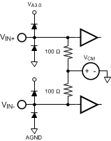 |
Differential analog input pins Each input pin is terminated to the internal common mode reference with a resistor for an internal differential termination. External resistors that terminate to the common-mode voltage bias are recommended but not strictly required. The total recommended differential resistive termination (including the internal 200 Ω termination) is recommended to be between 50 Ω and 200 Ω. |
| VIN– | 4 | ||
| Exposed thermal pad | Exposed thermal pad The exposed pad must be connected to the AGND ground plane electrically and with good thermal dissipation properties to achieve rated performance. |
||