TIDUES0E June 2019 – April 2024 TMS320F28P550SJ , TMS320F28P559SJ-Q1
- 1
- Description
- Resources
- Features
- Applications
- 6
- 1System Description
- 2System Overview
- 3Circuit Description
- 4Hardware, Software, Testing Requirements, and Test Results
- 5Design Files
- 6Related Documentation
- 7Terminology
- 8About the Author
- 9Revision History
4.4.4 Lab 4
- Test Setup for Lab 4 (Closed Current Loop -
Isec)
Compile the project by selecting Lab 4: Closed Loop Current with Resistive Load in the drop-down menu of Project Options from PowerSUITE GUI. Make sure current and voltage limits are set per operating conditions.
#if DAB_LAB == 4 #define DAB_CONTROL_RUNNING_ON C28X_CORE #define DAB_POWER_FLOW DAB_POWER_FLOW_PRIM_SEC #define DAB_INCR_BUILD DAB_CLOSED_LOOP_BUILD #define DAB_TEST_SETUP DAB_TEST_SETUP_RES_LOAD #define DAB_PROTECTION DAB_PROTECTION_ENABLED #define DAB_CONTROL_MODE DAB_CURRENT_MODE #define DAB_SFRA_TYPE 1 #define DAB_SFRA_AMPLITUDE (float32_t)DAB_SFRA_INJECTION_AMPLITUDE_LEVEL1 #endif- Run the project by clicking the green run button in CCS.
- Populate the required
variables in the watch window by loading JavaScript
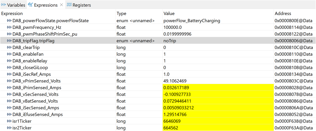
setupdebugenv_lab4.jsin the scripting console. Figure 4-37 Lab 4 Watch
View Configuration
 - Enable fans and relays by
writing "1" into
DAB_enableFanandDAB_enableRelay. - Enable PWM by writing “1”
to the
DAB_clearTripvariable. - In the watch view, check
if the
DAB_vPrimSensed_Volts,DAB_iPrimSensed_Amps,DAB_vSecSensed_Volts, andDAB_iSecSensed_Ampsvariables are updating periodically. - Set the output current by
writing to
DAB_iSecRef_Amps(in this example 1Adc). - Enable closed loop
operation by writing “1” to the
DAB_closeGiLoopvariable. The controller automatically adjusts the phase shift depending upon the operating conditions to generate secondary output current to match with that ofDAB_iSecRef_Amps.Note: In the software, the maximum phase shift is limited to 0.13 as a safety precaution. Please adjust the primary voltage to stay within the phase shift limits and still generate the required secondary current. - Now, slowly increase the
input VPRIM DC voltage and adjust
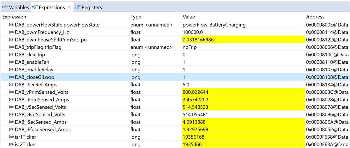
DAB_iSecRef_Ampsaccordingly to reach to the required operating point. Figure 4-38 Lab 4 -
Expression Window Closed Current LoopCAUTION: Make sure the secondary current is limited to a safe value depending upon the output load. High-impedance load can lead to dangerous secondary voltage which can destroy the board. Make sure secondary overvoltage protection is enabled and the threshold is set to a safe value.
Figure 4-38 Lab 4 -
Expression Window Closed Current LoopCAUTION: Make sure the secondary current is limited to a safe value depending upon the output load. High-impedance load can lead to dangerous secondary voltage which can destroy the board. Make sure secondary overvoltage protection is enabled and the threshold is set to a safe value.#define DAB_PROTECTION DAB_PROTECTION_ENABLED #define DAB_VSEC_TRIP_LIMIT ((float32_t)500) #define DAB_BOARD_PROTECTION_VSEC_OVERVOLTAGE 1
- Frequency response of closed loop current
- Run the SFRA by clicking on the SFRA icon. The SFRA GUI opens.
- Select the options for the device on the SFRA GUI; for example, for F280039, select floating point. Click the Setup Connection button. In the pop-up window, uncheck the boot-on-connect option and select an appropriate COM port. Select the OK button. Return to the SFRA GUI and click Connect.
- The SFRA GUI connects to the device. A SFRA
sweep can now be started by clicking Start Sweep. The complete
SFRA sweep takes a few minutes to finish. Monitor the activity in the
progress bar on the SFRA GUI or by checking the flashing blue LED on the
back of the control card, which indicates UART activity.
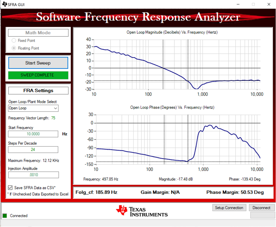
The plot in Figure 4-39 is captured with the PI compensator (gain of 0.5).
 Test condition: VIN= 800 V, VOUT = 500 V, IOUT = 10 A, SFRA amplitude = 0.002Figure 4-39 Lab 4 SFRA Open Loop Plot for the Closed Current Loop
#define DAB_GI_KP (float32_t) 0.5
#define DAB_GI_KI (float32_t) 0.0063030
#define DAB_GI_UMAX (float32_t) 0.13
#define DAB_GI_UMIN (float32_t) -0.13
#define DAB_GI_IMAX (float32_t) 2.0
#define DAB_GI_IMIN (float32_t) -2.0