TIDUES0E June 2019 – April 2024 TMS320F28P550SJ , TMS320F28P559SJ-Q1
- 1
- Description
- Resources
- Features
- Applications
- 6
- 1System Description
- 2System Overview
- 3Circuit Description
- 4Hardware, Software, Testing Requirements, and Test Results
- 5Design Files
- 6Related Documentation
- 7Terminology
- 8About the Author
- 9Revision History
4.4.3 Lab 3
In Lab 3, the converter is run in secondary
voltage close-loop configuration (DAB_vSecSensed_Volts).
This lab runs the voltage mode compensator, obtains the open-loop transfer function of plant from SFRA, and runs the design compensator for the plant in the compensator design tool.
Launch the compensation designer which prompts the selection of a valid SFRA data file. Import the SFRA data from the run in Lab 2 into the compensation designer to design a 2P2Zcompensator. Keep more margins during this iteration of the design to make sure that when the loop is closed, the system is stable. The following coefficient values are hard-coded in the software. The compensation designer GUI gives information about the stability of the loop, gain margin, phase margin, and bandwidth of the loop. The coefficients can be modified in the compensation designer GUI.
#define DAB_GV_2P2Z_A1 ((float32_t) -1.8756666)
#define DAB_GV_2P2Z_A2 ((float32_t) 0.8756666)
#define DAB_GV_2P2Z_B0 (float32_t) 1.4329852)
#define DAB_GV_2P2Z_B1 ((float32_t) -2.7994568)
#define DAB_GV_2P2Z_B2 (float32_t) 1.3664965)- Test Setup for Lab 3 (Closed
Voltage Loop - Sec)
Compile the project by selecting Lab 3: Closed Loop Voltage with Resistive Load in the drop-down menu of Project Options from PowerSUITE GUI. Make sure current and voltage limits are set per operating conditions.
#if DAB_LAB == 3
#define DAB_CONTROL_RUNNING_ON C28X_CORE
#define DAB_POWER_FLOW DAB_POWER_FLOW_PRIM_SEC
#define DAB_INCR_BUILD DAB_CLOSED_LOOP_BUILD
#define DAB_TEST_SETUP DAB_TEST_SETUP_RES_LOAD
#define DAB_PROTECTION DAB_PROTECTION_ENABLED
#define DAB_CONTROL_MODE DAB_VOLTAGE_MODE
#define DAB_SFRA_TYPE 2
#define DAB_SFRA_AMPLITUDE (float32_t)DAB_SFRA_INJECTION_AMPLITUDE_LEVEL2
#endif
Use the following steps to run voltage close loop:
- Run the project by clicking the green run button in CCS.
- Populate the required
variables in the watch window by loading JavaScript
setupdebugenv_lab3.jsin the scripting console.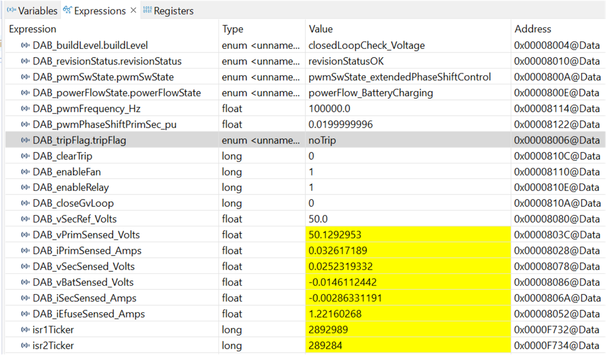 Figure 4-32 Lab 3 - Watch
View Configuration
 - Enable fans and relays by
writing "1" into
DAB_enableFanandDAB_enableRelay. - Enable PWM by writing “1”
to the
DAB_clearTripvariable. - In the watch view, check
if the
DAB_vPrimSensed_Volts,DAB_iPrimSensed_Amps,DAB_vSecSensed_Volts, andDAB_iSecSensed_Ampsvariables are updating periodically. - Set the output voltage by
writing to
DAB_vSecRef_Volts(in this example 50Vdc). - Enable closed loop
operation by writing “1” to the
DAB_closeGvLoopvariable. The controller automatically adjusts the phase shift , depending upon the operating conditions to generate secondary output voltage to match with that ofDAB_vSecRef_Volts.Note: In the software the maximum phase shift is limited to 0.13 as a safety precaution. Adjust the primary voltage to stay within the phase shift limits and still generate the required secondary voltage. - Slowly increase the input
VPRIM DC voltage and adjust
DAB_vSecRef_Voltsaccordingly, to reach to the required operating point. - Test the closed-loop
operation by varying
DAB_vSecRef_Voltsfrom 400 V to 500 V. Observe that theDAB_vSecSensed_Voltstracks this command reference.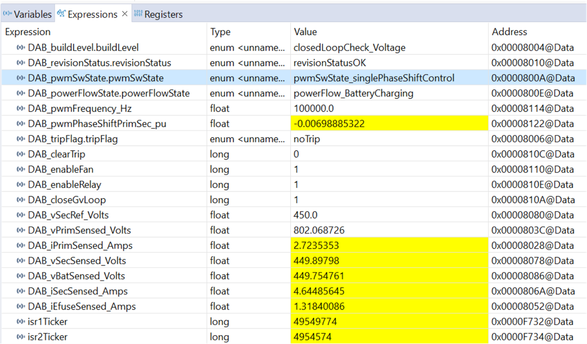 Figure 4-33 Lab 3 - Closed
Voltage Loop Expression Window
 - The control scheme can be
changed between single phase shift SPS and extended phase shift EPS, by
selecting the according variable in the DAB_pwmSwState.pwmSwState
drop down. Figure 4-34 shows that secondary side is hard-switching in this condition with SPS control.
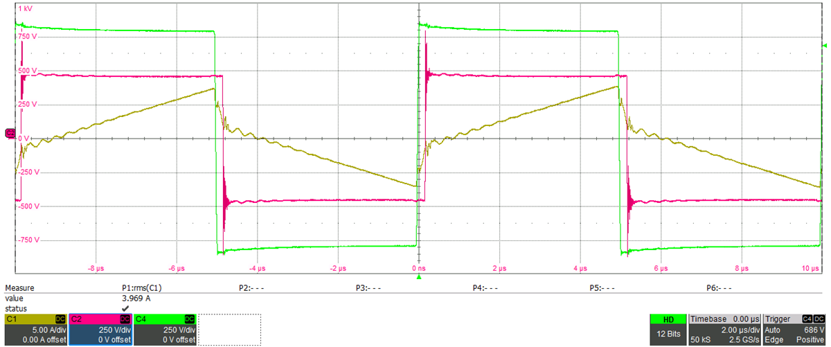 Primary side switch node voltage (green), secondary side switch node voltage (red), inductor current (yellow)Figure 4-34 Lab 3 - Waveforms in Single Phase Shift Control (SPS)
Test condition: VIN = 800 V, VOUT = 450 V, IOUT = 6.5 A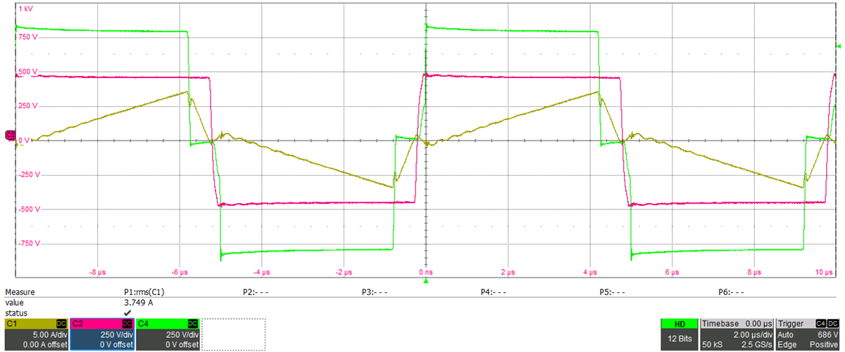 Primary side switch node voltage (green), secondary side switch node voltage (red), inductor current (yellow)Figure 4-35 Lab 3 - Waveforms in Extended Phase Shift Control (EPS)
Test condition: VIN = 800 V, VOUT = 450 V, IOUT = 6.5 AThe additional phase shift on the primary side introduced with EPS control is seen in Figure 4-35. Here both the primary side and the secondary side are soft-switching.
- Frequency response of closed loop voltage
- Run the SFRA by clicking on the SFRA icon. The SFRA GUI opens.
- Select the options for the device on the SFRA GUI; for example, for F280039, select floating point. Click the Setup Connection button. In the pop-up window, uncheck the boot-on-connect option and select an appropriate COM port. Select the OK button. Return to the SFRA GUI and click the Connect button.
- The SFRA GUI connects to
the device. An SFRA sweep can now be started by clicking the Start
Sweep button. The complete SFRA sweep takes a few minutes to
finish. Monitor the activity in the progress bar on the SFRA GUI or by
checking the flashing blue LED on the back of the control card, which
indicates UART activity.
The bode plot in Figure 4-36 is captured using a DF22 compensator.
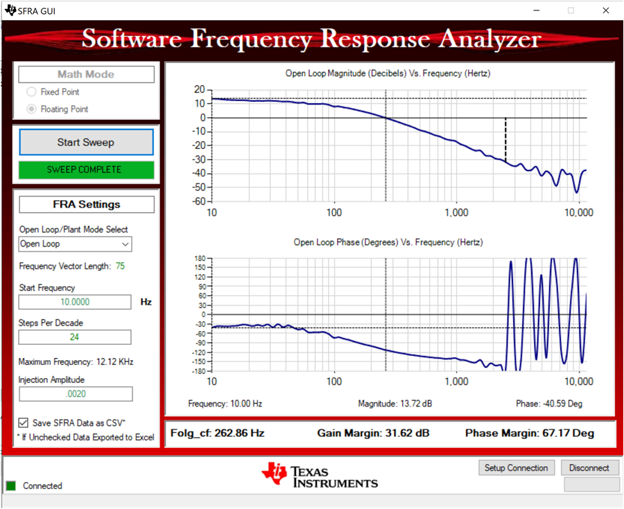 Test condition: VIN= 800 V, VOUT = 500 V, IOUT = 10 A, SFRA amplitude = 0.002Figure 4-36 Lab 3 - SFRA Open Loop Plot for the Closed Voltage Loop