SLOA198A September 2014 – December 2021 DRV2665 , DRV2667 , DRV2700 , DRV8662
- Trademarks
- 1 Boost Converter Basics
- 2 DRV8662, DRV2700, DRV2665, and DRV2667 Boost Converter
- 3 Configuring the Boost Converter
- 4 Boost Converter Output Voltage
- 5 Calculating the Load Current
- 6 Selecting an Inductor
- 7 Calculate the Maximum Boost Current
- 8 Output Capacitor Selection
- 9 Input Capacitor Selection
- 10PCB Layout
- 11Examples
- 12Revision History
10 PCB Layout
Use the following guidelines for PCB layout.
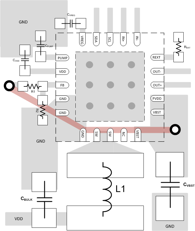
- Place the feedback resistors, R1 and R2, close to the FB pin. If the resistors are placed far from the FB pin, then noise can enter the FB trace and causes instability or unwanted ripple.
- Protect the feedback trace (Red trace). Isolate the feedback trace on a different layer and shield from the SW node using a ground plane.
- Minimize the size of SW node trace. The trace between the SW pins and the inductor terminal should be as physically small as possible. A large switch node can add parasitic capacitance and slow the switching frequency of the boost converter, preventing it from delivering the required current. A small SW node also helps prevent radiated emissions.
- Place the bulk input capacitor near the inductor. The bulk input capacitor provides the current during quick transient current spikes. Closer means less resistance between the bulk capacitor and inductor.
- Place the output capacitor near the VBST pin.