SLOA198A September 2014 – December 2021 DRV2665 , DRV2667 , DRV2700 , DRV8662
- Trademarks
- 1 Boost Converter Basics
- 2 DRV8662, DRV2700, DRV2665, and DRV2667 Boost Converter
- 3 Configuring the Boost Converter
- 4 Boost Converter Output Voltage
- 5 Calculating the Load Current
- 6 Selecting an Inductor
- 7 Calculate the Maximum Boost Current
- 8 Output Capacitor Selection
- 9 Input Capacitor Selection
- 10PCB Layout
- 11Examples
- 12Revision History
11.1.3 Boost Performance Results
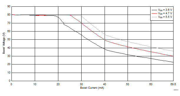
The actual load regulation and boost efficiency for the DRV8662EVM are shown in Figure 11-2. The load regulation is a measure of the boost voltage versus the boost output current. In Figure 11-2, the voltage regulation begins to drop above approximately 31 mA of boost output current.
 Figure 11-2 Actual Load Regulation and Boost Efficiency
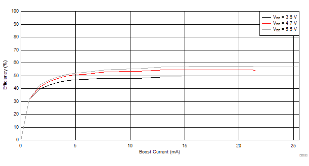
The boost efficiency is shown in Figure 11-3. The efficiency data was removed after the boost voltage decreased by more than 5 V.
 Figure 11-3 Boost Efficiency