SLOA198A September 2014 – December 2021 DRV2665 , DRV2667 , DRV2700 , DRV8662
- Trademarks
- 1 Boost Converter Basics
- 2 DRV8662, DRV2700, DRV2665, and DRV2667 Boost Converter
- 3 Configuring the Boost Converter
- 4 Boost Converter Output Voltage
- 5 Calculating the Load Current
- 6 Selecting an Inductor
- 7 Calculate the Maximum Boost Current
- 8 Output Capacitor Selection
- 9 Input Capacitor Selection
- 10PCB Layout
- 11Examples
- 12Revision History
10.1 What to Avoid: Incorrect Inductor Placement
In space-constrained applications, PCB real estate often trumps correct component placement. While layout guidelines were provided in the previous section, this section specifically covers inductor placement in more detail. The inductor should be placed as close to the SW node as possible; this helps reduce parasitic resistances, inductances, and most importantly, parasitic capacitances.
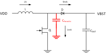
 Figure 10-1 SW Node Parasitic Capacitance
What happens if the SW node has too much parasitic capacitance? Two things:
- The switching frequency decreases due to a higher RC constant, resulting in less current delivery to the load
- The SW node stores charge in the parasitic capacitor, resulting in less current delivery to the load
The switching frequency changes as a result of the charging and discharging of the parasitic capacitor each cycle. Figure 10-2 shows how the current charge cycle of the inductor changes when parasitic capacitance is present.
 Figure 10-2 Inductor
Charging with Parasitic Capacitance
Figure 10-2 Inductor
Charging with Parasitic CapacitanceFigure 10-2 shows that the period of the inductor charge cycle increases with parasitic capacitance. This longer charge cycle results in a slower boost-switching frequency.
In addition to a slower switching frequency, the parasitic capacitance on the SW node consumes charge. If, for example, the DRVxxxx boost design normally supports 10-mA current and there is parasitic capacitance present, a significant portion – sometimes up to 1 mA of the current – can be consumed by the parasitic capacitance. This means that 10% of the current intended for the load is being consumed by the parasitic capacitance.
Both of these issues can have drastic effects on the output waveform. To identify switch node parasitic capacitance, look for continuous switching on the SW pin. During normal operation, the switching turns on and off depending on the current required; however, with parasitic capacitance the SW node often continuously switches to recover for lost switch cycles and current.