ZHCSFI3B August 2016 – May 2019 UCD90320
PRODUCTION DATA.
- 1 特性
- 2 应用
- 3 说明
- 4 修订历史记录
- 5 说明 (续)
- 6 Pin Configuration and Functions
- 7 Specifications
-
8 Detailed Description
- 8.1 Overview
- 8.2 Functional Block Diagram
- 8.3 Feature Description
- 8.4
Device Functional Modes
- 8.4.1 Rail Monitoring Configuration
- 8.4.2 GPI Configuration
- 8.4.3 Rail Sequence Configuration
- 8.4.4 Fault Responses Configuration
- 8.4.5 GPO Configuration
- 8.4.6 Margining Configuration
- 8.4.7 Pin Selected Rail States Configuration
- 8.4.8 Watchdog Timer
- 8.4.9 System Reset Function
- 8.4.10 Cascading Multiple Devices
- 8.4.11 Rail Monitoring
- 8.4.12 Status Monitoring
- 8.4.13 Data and Error Logging to EEPROM Memory
- 8.4.14 Black Box First Fault Logging
- 8.4.15 PMBus Address Selection
- 8.4.16 ADC Reference
- 8.4.17 Device Reset
- 8.4.18 Brownout
- 8.4.19 Internal Fault Management
- 8.5 Device Configuration and Programming
- 9 Application and Implementation
- 10Power Supply Recommendations
- 11Layout
- 12器件和文档支持
- 13机械、封装和可订购信息
8.4.5.2 Logic GPO
UCD90320 also has 16 dedicated Logic GPO (LGPO) pins. The configuration window is under Pin Assignment tab, as shown in Figure 19.
 Figure 19. Logic GPO Configuration Window (Hardware Configure ► Monitor and GPIO Pins Assignment)
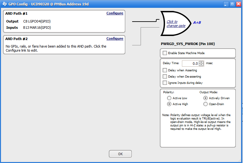
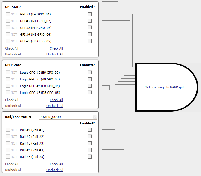
 Each LGPO is controlled by an internal Boolean logic builder. Figure 20 shows the configuration interface of the Boolean logic builder. As shown, each Boolean logic builder has a top-level logic gate, which can be configured as AND, OR, or NOR gate with optional time delay. The inputs of the top-level logic gate are two AND paths. Each AND path can select a variety of inputs including GPI states, LGPO states, and rail statuses, as shown in Figure 21. The selectable rail statuses are summarized in Table 3. In Table 3, _LATCH type statuses stay asserted until cleared by a MFR PMBus command or by a specially configured GPI pin shown in Figure 12. See the UCD90320 Sequencer and System Health Controller PMBus Command Reference for complete definitions of rail-status types.
 Figure 20. Boolean Logic Builder Interface
  Figure 21. AND Path Configuration
 Table 3. Selectable Rail Statuses in Boolean Logic Builder
| Rail-Status Types | ||
|---|---|---|
| POWER_GOOD | IOUT_OC_FAULT | TON_MAX_FAULT |
| MARGIN_EN | IOUT_OC_WARN | TOFF_MAX_WARN |
| MRG_LOW_nHIGH | IOUT_UC_FAULT | TON_MAX_FAULT_LATCH |
| VOUT_OV_FAULT | IOUT_OC_FAULT_LATCH | TOFF_MAX_WARN_LATCH |
| VOUT_OV_WARN | IOUT_OC_WARN_LATCH | SEQ_ON_TIMEOUT |
| VOUT_UV_WARN | IOUT_UC_FAULT_LATCH | SEQ_OFF_TIMEOUT |
| VOUT_UV_FAULT | TEMP_OT_FAULT | SEQ_ON_TIMEOUT_LATCH |
| VOUT_OV_FAULT_LATCH | TEMP_OT_WARN | SEQ_OFF_TIMEOUT_LATCH |
| VOUT_OV_WARN_LATCH | TEMP_OT_FAULT_LATCH | SYSTEM_WATCHDOG_TIMEOUT |
| VOUT_UV_WARN_LATCH | TEMP_OT_WARN_LATCH | SYSTEM_WATCHDOG_TIMEOUT_LATCH |
| VOUT_UV_FAULT_LATCH | SINGLE_EVENT_UPSET | |
The POWER_GOOD status used by GPO evaluation is based on actual monitoring result from AMON or DMON pins. For a rail that does not have a voltage monitor pin, the POWER_GOOD status is used by sequencing purpose only, and is not used by GPO evaluation. Therefore during GPO evaluation, a rail without an AMON or DMON pin never reports POWER_GOOD status.
Each LGPO can be also configured as a simple state machine, as shown in Figure 16. In state machine mode, the top-level logic gate is omitted and only one of the two AND paths is evaluated. The output of the state machine is the result of the active AND path. The evaluation initially starts with AND Path #1. If the evaluation result is TRUE, AND Path #1 remains active until its evaluation result becomes FALSE. When the output associates with AND Path#1 becomes FALSE, AND Path #2 becomes active in the next evaluation cycle. AND Path #2 remains active until its evaluation result becomes TRUE, then AND Path #1 becomes active in the next evaluation cycle. An evaluation cycle is triggered when any input signal to the state machine changes state.
GPO1 to GPO8 outputs are internally synchronized to the same clock edge to enable them to change states together. GPO9 to GPO16 outputs are internally synchronized to enable them to change states together. GPO1 through GPIO8 and GPO9 through GPIO16 outputs status are updated within an time window between approximately 1 µs and 3 µs.