ZHCSBQ3B October 2013 – July 2014 TPS92411
PRODUCTION DATA.
- 1 特性
- 2 应用
- 3 说明
- 4 修订历史记录
- 5 Pin Configuration and Functions
- 6 Specifications
- 7 Detailed Description
- 8 Application and Implementation
- 9 Power Supply Recommendations
- 10Layout
- 11器件和文档支持
- 12机械封装和可订购信息
封装选项
机械数据 (封装 | 引脚)
散热焊盘机械数据 (封装 | 引脚)
- DDA|8
订购信息
8 Application and Implementation
8.1 Application Information
The TPS92411 is an advanced, floating driver specifically designed for use with a linear regulator in low-power offline LED lighting applications. It integrates an on-board 100-V MOSFET switch to shunt LED current as the line transitions. As the line transitions through the cycle, the device monitors critical nodes for zero cross at which time the internal switch is either opened or shorted to steer the current through or away from the LED stack. Use the following design procedure to select components for the TPS92411. The following calculators may also be used to select components for the TPS92411:
- SLVC579 for 120-V applications using the TPS92410
- SLVC580 for 230-V applications using the TPS92410
- SLVC516 for 120-V applications using a discrete linear regulator
- SLVC517 for 230-V applications using a discrete linear regulator
PSpice and TINA-TI models are also available. The following are typical applications using the TPS92411 for both 120-V and 230-V applications using a discrete linear regulator.
8.2 Typical Application
8.2.1 120-VAC, Phase Dimmable 11.5-W Input with Discrete Linear Regulator
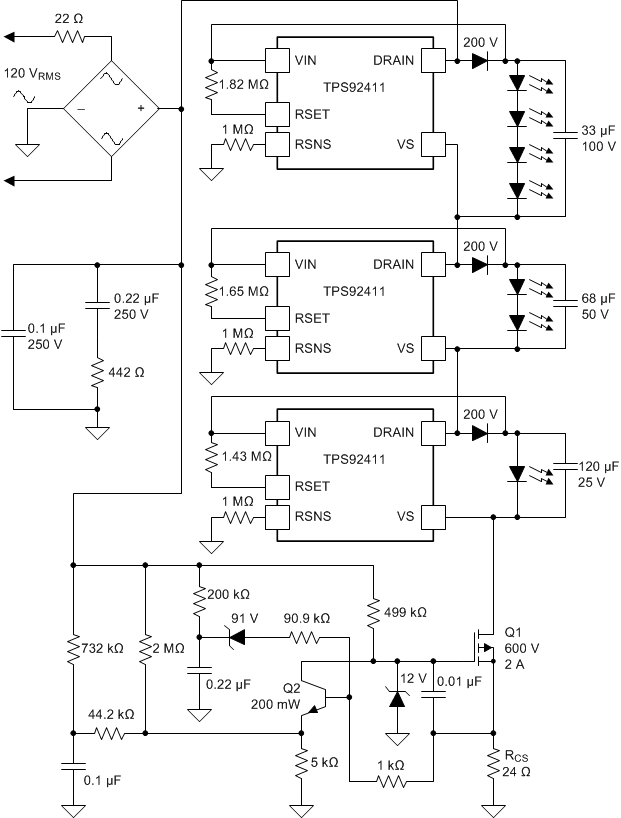 Figure 10. 120-VAC, Phase Dimmable 11.5-W Input with Discrete Linear Regulator
8.2.1.1 Design Requirements
For the 120-V application shown in Figure 10 the highest efficiency is obtained by using a high-voltage total LED stack to reduce losses in the linear regulator FET. The best current sharing efficiency between stacks can be achieved by using the lowest voltage stack at the bottom and making each stack voltage above 2 times the voltage of the stack below it. In this example 20-V LEDs are used. This effectively gives the lowest stack a total of 20 V, the middle stack a total of 40 V, and the upper stack a total of 80 V. The RSNS resistor is used to set a low voltage point so that when the VS pin voltage falls below this threshold (either from the AC line falling or a higher voltage stack switch above it turning OFF) the TPS92411 switch turns ON and bypasses the LEDs. During the ON-time, the LEDs are supplied current from the capacitor. The RSET voltage is used to set a threshold to detect when the input voltage crosses this threshold it turns OFF the switch and allows the LEDs to conduct current from the line and charge the bypass capacitor.
8.2.1.2 Detailed Design Procedure
- Set VRSNS for all three TPS92411 devices at 4 V
- Set VRSET for the bottom stack at 26 V (20 V stack plus 6 V headroom)
- Set VRSET for the middle stack at 46 V (40 V stack plus 6 V headroom)
- Set VRSET for the top stack at 86 V (80 V stack plus 6 V headroom)
Switching order as the rectified AC line voltage increases is shown in Table 1. Figure 11 illustrates when each switch turns ON or OFF.
8.2.1.2.1 Setting the Switching Thresholds (RSNS, RSET)
The TPS92411 features two threshold settings to allow for proper LED control. The first setting determines when the internal switch turns off and allows current to charge the capacitor and flow through the LEDs. The second setting determines when the switch turns on to shunt the LEDs and allow the capacitor to supply current. The lower switch turn-on threshold (VSNS) should be set first using a resistor (RRSNS) from the RSNS pin to system ground. For best efficiency set this threshold between 4 V and 6 V. Then the upper switch turn-off threshold (VVS) can be set using a resistor (RRSET) from the RSET pin to the VIN pin. Set this threshold approximately 6 V to 10 V above the LED stack voltage (VLED). The RSET threshold should be greater than the LED stack voltage plus the value of the RSNS threshold to prevent errant switching. These thresholds can be set with resistance calculated using Equation 1 and Equation 2.
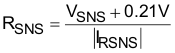
Table 1. Switching Order on Rising Edge of Rectified 120-VAC (1)(2)
| STACK | ||
|---|---|---|
| TOP 80-V | MIDDLE 40-V | BOTTOM 20-V |
| 0 | 0 | 0 |
| 0 | 0 | 1 |
| 0 | 1 | 0 |
| 0 | 1 | 1 |
| 1 | 0 | 0 |
| 1 | 0 | 1 |
| 1 | 1 | 0 |
| 1 | 1 | 1 |
 Figure 11. Switching Order on Rectified 120-VAC Waveform
The linear regulator in Figure 11 generates a current sense RMS voltage of approximately 2.3 V. The linear regulator RMS current is equal to the input current drawn from the AC line. For example, for a 11.5-W input power system the input current should be approximately 0.095 A and a 24-Ω resistor should be chosen for RCS. Other input power levels (PIN) can be obtained using Equation 3.
8.2.1.3 Application Curve
 Figure 12. Power Factor vs. Input Voltage
8.2.2 230-VAC, Phase Dimmable 16-W Input with Discrete Linear Regulator
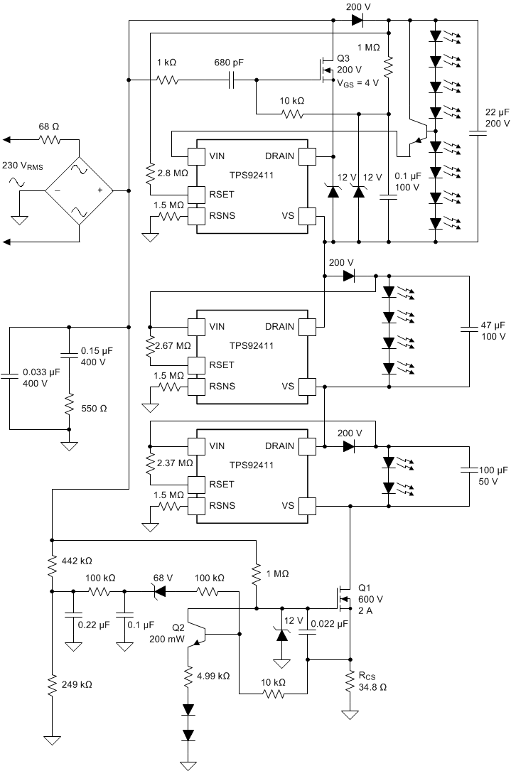 Figure 13. 230-VAC, Phase Dimmable 16-W Input with Discrete Linear Regulator
8.2.2.1 Design Requirements
In the 230-V application shown in Figure 13, the highest efficiency can be obtained by using a high-voltage total LED stack to reduce losses in the linear regulator FET. The best current sharing between stacks can be achieved by using the lowest voltage stack at the bottom and making each stack voltage above that two times that of the stack below it (as in described in the 120-V application). In this example, very good results can be obtained by setting the lowest stack at 40 V, the middle stack at 80 V, and adding a high-voltage cascode FET with the top stack and using 160 V. Use the RSNS pin to set a low voltage point so that when the VS pin of the device falls below this threshold (either from the AC line falling or a higher voltage stack switch above it turning OFF) the TPS92411 switch turns ON and bypasses the LEDs. During the ON-time, the capacitor supplies current to the LEDs. The RSET voltage threshold for a 230-V application is generally set to approximately 8 V to 12 V above the LED stack voltage connected across the TPS92411 (for an RSNS voltage of 6 V). This threshold is higher than in the typical 120-V application to allow more headroom.
8.2.2.2 Detailed Design Procedure
- Set VRSNS for all three TPS92411 devices at 6 V
- Set VRSET for the bottom stack at 49 V (40 V stack plus 9 V headroom)
- Set VRSET for the middle stack at 89 V (80 V stack plus 9 V headroom)
- Set VRSET for the top stack at 169 V (160 V stack plus 9 V headroom)
Switching order as the rectified AC line voltage increases is shown in Table 2. Figure 14 illustrates when each switch turns ON or OFF.
Table 2. Switching Order on Rising Edge of the Rectified 230-VAC Waveform(1)(2)
| STACK | ||
|---|---|---|
| TOP 160-V | MIDDLE 80-V | BOTTOM 40-V |
| 0 | 0 | 0 |
| 0 | 0 | 1 |
| 0 | 1 | 0 |
| 0 | 1 | 1 |
| 1 | 0 | 0 |
| 1 | 0 | 1 |
| 1 | 1 | 0 |
| 1 | 1 | 1 |
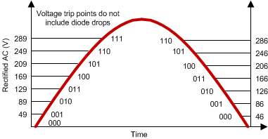 Figure 14. Switching Order on Rising Edge of the Rectified 230-VAC Waveform
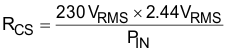
The linear regulator in Figure 14 generates a current sense RMS voltage of 2.44 V. The linear regulator RMS current is equal to the input current drawn from the AC line. For example, for a 16-W input power system the input current should be approximately 0.07 A and a 34.8-Ω resistor should be chosen for RCS. Other input power levels (PIN) can be calculated using Equation 4.
8.2.2.3 Application Curve
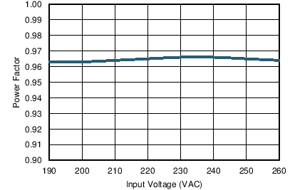 Figure 15. Power Factor Input Voltage