ZHCSBQ3B October 2013 – July 2014 TPS92411
PRODUCTION DATA.
- 1 特性
- 2 应用
- 3 说明
- 4 修订历史记录
- 5 Pin Configuration and Functions
- 6 Specifications
- 7 Detailed Description
- 8 Application and Implementation
- 9 Power Supply Recommendations
- 10Layout
- 11器件和文档支持
- 12机械封装和可订购信息
封装选项
机械数据 (封装 | 引脚)
散热焊盘机械数据 (封装 | 引脚)
- DDA|8
订购信息
7 Detailed Description
7.1 Overview
The TPS92411 is an advanced, floating driver specifically designed for use with a linear regulator in low-power offline LED lighting applications. It integrates an on-board 100-V MOSFET switch to shunt LED current as the line transitions. As the line transitions through the cycle, the device monitors critical nodes for zero cross at which time the internal switch is either opened or shorted to steer the current through or away from the LED stack. The TPS92411 does not directly control output power or LED current, it just directs current to the LED stack or bypasses the LED stack.
7.2 Functional Block Diagram
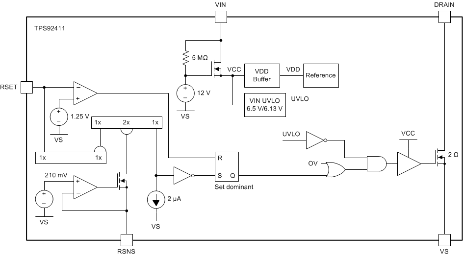 Figure 8. TPS92411 Block Diagram
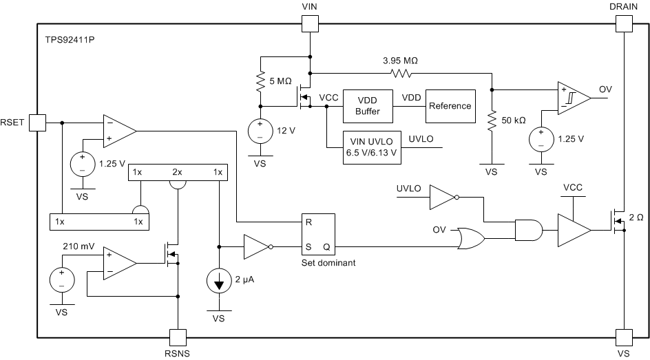 Figure 9. TPS92411P Block Diagram
7.3 Feature Description
7.3.1 Overvoltage Protection (OVP)
Overvoltage protection (OVP) in the TPS92411P version protects the device as well as the LEDs and storage capacitor. The OVP is set at approximately 100 V (VVIN – VVS) and closes the internal switch when the threshold voltage is reached. For this reason LED stack voltages of 94 V or less are recommended. Higher voltages can be used with the TPS92411 version but tolerances must be considered to ensure that the 105 V absolute maximum rating is not exceeded.
7.3.2 Input Undervoltage Lockout (UVLO)
The TPS92411 includes input UVLO. The UVLO prevents the device from operation until the VIN pin voltage with respect to VS exceeds 6.5 V and ensures the device behaves properly when enabled.
7.3.3 LED Capacitor
A capacitor is required across each LED stack to provide current to the LEDs during the switch ON time. Refer to the available calculator software (SLVC516 for 120-V applications or SLVC517 for 230-V applications) for calculating the minimum value required for any particular application. The software calculates the minimum value required for a particular application, but best performance is acheived by using as much capacitance as possible given size and cost constraints. These design tools also calculate a minimum value for any given current ripple percent or flicker index desired for the particular application.
7.3.4 Blocking Diode
A blocking diode is required between the drain of the switch (DRAIN) and the anode of the LED stack. This prevents the LED capacitor from discharging through the switch during the switch ON time instead allowing it to discharge through the LED stack. This diode should be rated for 200 V reverse voltage and capable of forward currents as high as the average linear regulator current setting.
7.4 Device Functional Modes
The TPS92411P has 4 functional modes while the TPS92411 has 3:
7.4.1 Input UVLO
As described in the previous section the device and internal switch will remain off until VIN is 6.5V or greater with respect to VS.
7.4.2 Operating with Internal Switch ON
After the device crosses the UVLO threshold the internal switch will turn on and remain on until the voltage at the VIN pin exceeds the threshold voltage set by the RSET resistor.
7.4.3 Operating with Internal Switch OFF
When the RSET threshold voltage is exceeded on the VIN pin the internal switch will turn off forcing all the current to flow through the LEDs and charge the LED capacitor. The switch will remain off until the VS pin drops below the threshold voltage set by RSNS or an overvoltage event occurs (TPS92411P only).
7.4.4 Overvoltage Operation (TPS92411P)
If an LED fails open or a string voltage exceeding the OVP level is used the device will enter OVP operation. The internal switch will close and remain closed until the VIN voltage with respect to the VS pin drops low enough to engage normal operation again.