ZHCSBQ3B October 2013 – July 2014 TPS92411
PRODUCTION DATA.
- 1 特性
- 2 应用
- 3 说明
- 4 修订历史记录
- 5 Pin Configuration and Functions
- 6 Specifications
- 7 Detailed Description
- 8 Application and Implementation
- 9 Power Supply Recommendations
- 10Layout
- 11器件和文档支持
- 12机械封装和可订购信息
封装选项
机械数据 (封装 | 引脚)
散热焊盘机械数据 (封装 | 引脚)
- DDA|8
订购信息
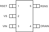
5 Pin Configuration and Functions
DDA (SO-8 Power-Pad) PACKAGE
8 PIN
(TOP VIEW)
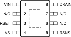
Pin Functions
| PIN | I/O | DESCRIPTION | ||
|---|---|---|---|---|
| NAME | NO. | |||
| DDA | DBV | |||
| DRAIN | 8 | 4 | O | Drain of the internal switch. |
| N/C | 2 | — | — | Not internally connected. |
| N/C | 6 | |||
| N/C | 7 | |||
| VIN | 1 | 3 | I | Positive power supply for the device. |
| VS | 4 | 2 | I/O | Source of the internal switch. This pin is also the device floating ground. |
| RSET | 3 | 1 | I/O | A resistor connected between the RSET pin and the VIN pin sets the rising threshold to open the switch. |
| RSNS | 5 | 5 | I/O | A resistor connected between the RSNS pin to system ground senses the VS voltage relative to system ground. |
| Exposed Themal Pad | Connect to VS pin directly beneath the device. | |||