ZHCSBQ3B October 2013 – July 2014 TPS92411
PRODUCTION DATA.
- 1 特性
- 2 应用
- 3 说明
- 4 修订历史记录
- 5 Pin Configuration and Functions
- 6 Specifications
- 7 Detailed Description
- 8 Application and Implementation
- 9 Power Supply Recommendations
- 10Layout
- 11器件和文档支持
- 12机械封装和可订购信息
封装选项
机械数据 (封装 | 引脚)
散热焊盘机械数据 (封装 | 引脚)
- DDA|8
订购信息
6 Specifications
6.1 Absolute Maximum Ratings
All voltages are with respect to VS, –40 °C < TJ = TA ≤ 150 °C. All currents are positive into and negative out of the specified terminal (unless otherwise noted).| MIN | MAX | UNIT | ||
|---|---|---|---|---|
| Supply voltage | VIN | –0.3 | 105 | V |
| Switch voltage | DRAIN | –0.3 | 105 | |
| Junction temperature | TJ | –40 | 165 | ºC |
6.2 Handling Ratings
| MIN | MAX | UNIT | |||
|---|---|---|---|---|---|
| Tstg | Storage temperature range | –65 | 150 | °C | |
| V(ESD) | Electrostatic discharge | Human body model (HBM), per ANSI/ESDA/JEDEC JS-001, all pins(1) | 1 | kV | |
| Charged device model (CDM), per JEDEC specification JESD22-C101, all pins(2) | 250 | V | |||
(1) JEDEC document JEP155 states that 500-V HBM allows safe manufacturing with a standard ESD control process.
(2) JEDEC document JEP157 states that 250-V CDM allows safe manufacturing with a standard ESD control process.
6.3 Recommended Operating Conditions
Over operating free-air temperature range (unless otherwise noted)| MIN | TYP | MAX | UNIT | |||
|---|---|---|---|---|---|---|
| VIN | Input voltage | TPS92411P | 7.5 | 94 | V | |
| TPS92411 | 7.5 | 100 | ||||
| TJ | Operating junction temperature | –40 | 25 | 150 | °C | |
6.4 Thermal Information
| THERMAL METRIC(1) | TPS92411 | UNIT | ||
|---|---|---|---|---|
| DBV | DDA | |||
| 5 PINS | 8 PINS | |||
| θJA | Junction-to-ambient thermal resistance(2) | 209.8 | 58.6 | °C/W |
| θJCtop | Junction-to-case (top) thermal resistance(3) | 125.2 | 72 | |
| θJB | Junction-to-board thermal resistance(4) | 38 | 39.1 | |
| ψJT | Junction-to-top characterization parameter(5) | 15.6 | 21.6 | |
| ψJB | Junction-to-board characterization parameter(6) | 37.1 | 39.1 | |
| θJCbot | Junction-to-case (bottom) thermal resistance(7) | N/A | 15 | |
(1) For more information about traditional and new thermal metrics, see the IC Package Thermal Metrics application report, SPRA953.
(2) The junction-to-ambient thermal resistance under natural convection is obtained in a simulation on a JEDEC-standard, high-K board, as specified in JESD51-7, in an environment described in JESD51-2a.
(3) The junction-to-case (top) thermal resistance is obtained by simulating a cold plate test on the package top. No specified JEDEC-standard test exists, but a close description can be found in the ANSI SEMI standard G30-88.
(4) The junction-to-board thermal resistance is obtained by simulating in an environment with a ring cold plate fixture to control the PCB temperature, as described in JESD51-8.
(5) The junction-to-top characterization parameter, θJT, estimates the junction temperature of a device in a real system and is extracted from the simulation data for obtaining θJA, using a procedure described in JESD51-2a (sections 6 and 7).
(6) The junction-to-board characterization parameter, θJB, estimates the junction temperature of a device in a real system and is extracted from the simulation data for obtaining θJA, using a procedure described in JESD51-2a (sections 6 and 7).
(7) The junction-to-case (bottom) thermal resistance is obtained by simulating a cold plate test on the exposed (power) pad. No specific JEDEC standard test exists, but a close description can be found in the ANSI SEMI standard G30-88.
6.5 Electrical Characteristics
Unless otherwise specified –40 °C ≤ TJ = TA ≤ 150 °C, (VVIN – VVS) = 30 V, RRSET = RRSNS = Open, all voltages are with respect to VS.| PARAMETER | TEST CONDITIONS | MIN | TYP | MAX | UNIT | ||
|---|---|---|---|---|---|---|---|
| INPUT SUPPLY (VIN) | |||||||
| VIN(ovp) | Input overvoltage protection | TPS92411P | Rising threshold | 95 | 100 | V | |
| Falling threshold | 96 | ||||||
| Hysteresis | 4 | ||||||
| IQ | Bias current | 200 | 400 | μA | |||
| VIN(uvlo) | Input undervoltage lockout | Rising threshold | 6.5 | 7 | V | ||
| VIN(hys) | Input UVLO hysteresis | 370 | mV | ||||
| SWITCH CONTROL (RSNS, RSET) | |||||||
| IRSNS | RSNS threshold current | –3.3 | –4 | –4.9 | μA | ||
| VRSNS_OS | RSNS offset voltage | 165 | 210 | 255 | mV | ||
| VRSET | RSET threshold voltage | 1.2 | 1.25 | 1.3 | V | ||
| IRSET | RSET current | IRSNS = –20 μA, (VRSET – VVS) = 1.5 V | –9.3 | –10 | –10.7 | μA | |
| IRSNS = –40 μA, (VRSET – VVS) = 1.5 V | –19 | –20 | –21 | ||||
| IRSNS = –100 μA, (VRSET – VVS) = 1.5 V | –47.9 | –50 | –52.1 | ||||
| SWITCH (DRAIN, VS) | |||||||
| RDS(on) | On-resistance | IDRAIN = 100 mA, TJ = 25°C | 1 | 2 | 2.5 | Ω | |
| dv/dt(ON) | Switch ON slew rate | (VDRAIN – VVS) falling 36 V to 4 V, ISW = 100 mA |
1 | V/μs | |||
| dv/dt(OFF) | Switch OFF slew rate | (VDRAIN – VVS) = rising 4 V to 36 V, ISW = 100 mA |
0.5 | ||||
6.6 Typical Characteristics
Unless otherwise stated, –40 °C ≤ TA = TJ ≤ 150 °C, (VVIN – VVS) = 30 V, all voltages are with respect to VS.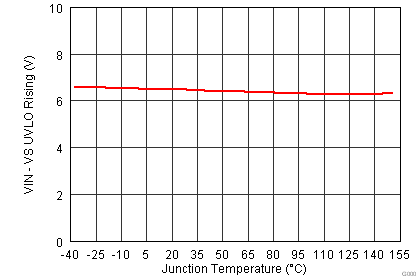 Figure 1. UVLO vs. Temperature
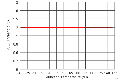 Figure 3. RSET Threshold vs. Temperature
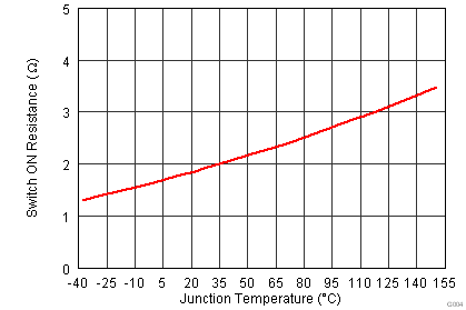 Figure 5. Switch On-Resistance (RDS(on)) vs. Temperature
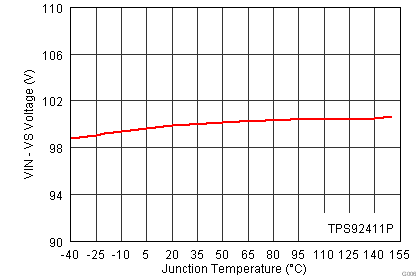 Figure 7. (VVIN – VVS) Overvoltage Threshold vs. Temperature
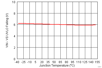 Figure 2. UVLO vs. Temperature
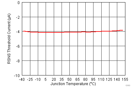 Figure 4. RSNS Threshold Current vs. Temperature
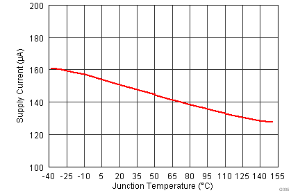 Figure 6. Input Voltage Quiescent Current vs. Temperature