ZHCSBQ3B October 2013 – July 2014 TPS92411
PRODUCTION DATA.
- 1 特性
- 2 应用
- 3 说明
- 4 修订历史记录
- 5 Pin Configuration and Functions
- 6 Specifications
- 7 Detailed Description
- 8 Application and Implementation
- 9 Power Supply Recommendations
- 10Layout
- 11器件和文档支持
- 12机械封装和可订购信息
封装选项
机械数据 (封装 | 引脚)
散热焊盘机械数据 (封装 | 引脚)
- DDA|8
订购信息
10 Layout
10.1 Layout Guidelines
The TPS92411 allows for a simple layout, however some considerations should be taken. The RSET resistor should be connected directly between the RSET pin and VIN pin as close to the device as possible. The trace between the resistor and the RSET pin should be as short as possible. The trace from the RSNS pin to the RSNS resistor should also be as short as possible to minimize parasitic capacitances. The blocking diode should be placed between the DRAIN pin and the VIN pin and also located close to the device. Placement of the LED capacitor may depend on the physical design of the application, however it should be placed as close to the TPS92411 as the design allows to minimize parasitic inductances.
10.2 Layout Example
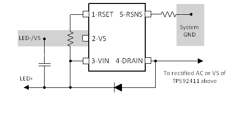 Figure 16. Recommended Component Placement (DBV)
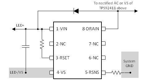 Figure 17. Recommended Component Placement (DDA)