ZHCSCM9 May 2014 TPS92410
PRODUCTION DATA.
- 1 特性
- 2 应用
- 3 说明
- 4 修订历史记录
- 5 Pin Configuration and Functions
- 6 Specifications
-
7 Detailed Description
- 7.1 Overview
- 7.2 Functional Block Diagram
- 7.3
Feature Description
- 7.3.1 Setting the Linear Regulator Current/Input Power (CS)
- 7.3.2 Over-Voltage Protecton (DOV)
- 7.3.3 Input Undervoltage Lockout (UVLO)
- 7.3.4 Reference Voltage (VREF)
- 7.3.5 Forward Phase Dimmer Detection (CPS, CDD)
- 7.3.6 Analog Dimming Input and Setting VCS (ADIM)
- 7.3.7 Thermal Foldback (TSNS)
- 7.3.8 Internal Regulator (VCC)
- 7.3.9 Error Amplifier (COMP)
- 7.3.10 Linear MOSFET Gate Drive (GDL)
- 7.3.11 EMI Filter
- 7.3.12 Thermal Shutdown
- 7.4 Device Functional Modes
- 8 Application and Implementation
- 9 Power Supply Recommendations
- 10Layout
- 11器件和文档支持
- 12机械封装和可订购信息
8 Application and Implementation
8.1 Application Information
The TPS92410 is a linear controller designed to be used in conjunction with the TPS92411 switch for high voltage off-line LED drive applications. Typical uses include 120 VAC and 230 VAC input LED drivers with either analog or phase dimming. However like any linear controller it may also be used with a DC input voltage up to 450 V. The following applications are for typical off-line LED drivers with 120 VAC and 230 VAC input voltages.
8.2 Typical Application
8.2.1 120-VAC Input, 6.6-W LED Driver
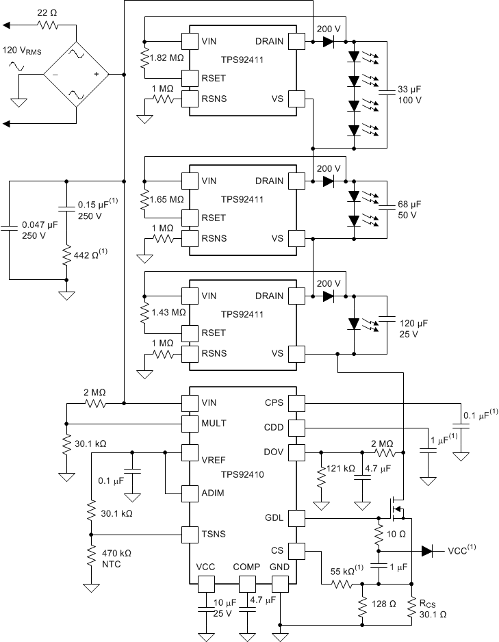
8.2.1.1 Design Requirements
This application requires a 6.6-W input power, high-efficiency, phase-dimmable LED lamp for use on 120-V systems.
8.2.1.2 Detailed Design Procedure
The TPS92411 components are chosen using the guidelines in the TPS92411 datasheet. Most of the values used for the TPS92410 are recommended values for any 120-V system. Connect the input voltage directly to the rectified AC while the MULT pin is connected to a 2-MΩ, 30.1-kΩ resistor divider from the rectified AC to ground. The VREF pin should have a 0.1-µF capacitor tied to ground for decoupling. The VCC pin should be decoupled using a 10-µF ceramic capacitor to ground and the COMP pin should have a 4.7-µF ceramic capacitor to ground. Connect a 0.1-µF ceramic capacitor from the CPS pin to ground. Connect a 1-µF ceramic capacitor from the CDD pin to ground to enable phase dimmable operation. This results in a 150 ms dimmer detect time constant. The over-voltage protection using the DOV pin can be set using Equation 3. In this case a MOSFET drain over-voltage level of approximately 27 V is chosen. A 4.7-µF capacitor should be placed in parallel with a 121-kΩ resistor from the DOV pin to ground to set a time constant and for filtering for all applications.
Choose RDRAIN for the appropriate voltage, in this case 2 MΩ is chosen. Connect a 10-Ω resistor in series with a 1-µF ceramic capacitor from GDL to CS for stability and to help reduce EMI. Place a diode from the center point of these two components to the VCC pin to clamp the voltage on the GDL pin and the CS pin that can become high with some forward phase dimmers. A rating of at least 20 V and 100 mA is recommended with a peak-repetitive current rating of at least 2 A. A 55-kΩ resistor should be connected between the MOSFET source and the CS pin for additional protection. Connect a 30.1-kΩ resistor from the TSNS pin to the VREF pin. The NTC thermistor to ground should be selected so that the desired foldback temperature results in a thermistor value of 30.1 kΩ. RCS is then calculated using Equation 1. RCS = 25 Ω is very close, a 30.1 Ω in parallel with a 182 Ω resulting in about 25.83 Ω was chosen.
Application Curves
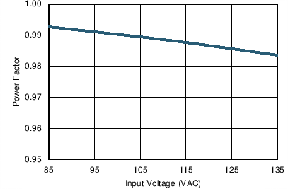
| 120VAC | Top stack = 80 V | 6.8 W Input |
| Middle stack = 40 V | Bottom stack= 20 V | VADIM = 1.5 V |
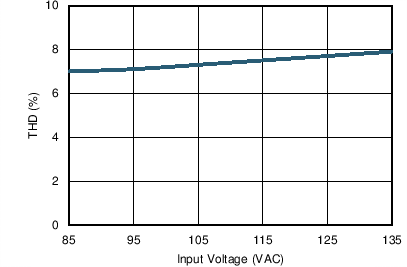
| 120VAC | Top stack = 80 V | 6.8 W Input |
| Middle stack = 40 V | Bottom stack= 20 V | VADIM = 1.5 V |
8.2.2 230-VAC Input, 11-W LED Driver
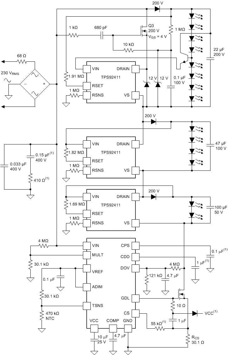
8.2.2.1 Design Requirements
This application requires a 11-W input power, high-efficiency, phase-dimmable LED lamp for use on 230-V systems.
8.2.2.2 Detailed Design Procedure
The TPS92411 components are chosen using the guidelines in the TPS92411 datasheet. Most of the values used for the TPS92410 are recommended values for any 230-V system. The input voltage should be connected directly to rectified AC while the MULT pin is connected to a 4-MΩ, 30.1-kΩ resistor divider between rectified AC and ground. The VREF pin should have a 0.1-µF capacitor connected to ground to provide decoupling. The VCC pin should be decoupled using a 10-µF ceramic capacitor to ground and the COMP pin should have a 4.7-µF ceramic capacitor to ground. Connect a 0.1-µF ceramic capacitor from the CPS pin to ground. Connect a 1-µF ceramic capacitor from CDD to ground to enable phase dimmable operation. This results in a 150 ms dimmer detect time constant. The over-voltage protection using the DOV pin can be set using Equation 3. This case includes a MOSFET drain over-voltage level of approximately 51 V. A 4.7-µF capacitor should be placed in parallel with a 121-kΩ resistor from the DOV pin to ground to set a time constant and for filtering for all applications.
Choose RDRAIN for the appropriate voltage, this case uses a value of 4-MΩ. A 10-Ω resistor in series with a 1-µF ceramic capacitor from GDL to CS adds stability and helps reduce EMI. A diode should be placed from the center point of these two components to the VCC pin to clamp the voltage on the GDL pin and the CS pin that can become high with some forward phase dimmers. A rating of at least 20 V and 100 mA is recommended with a peak-repetitive current rating of at least 2 A. A 55-kΩ resistor should be connected between the MOSFET source and the CS pin for additional protection. Connect a 30.1-kΩ resistor from the TSNS pin to the VREF pin. The NTC thermistor to ground should be selected so that the desired foldback temperature results in a thermistor value of 30.1 kΩ. RCS is then calculated using Equation 1. RCS = 30.1 Ω is very close and was chosen for this design.
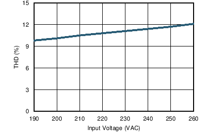
8.2.2.3 Application Curves
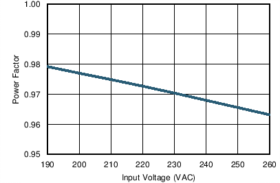
| Top stack = 160 V | 11.2 W Input | 230 VAC |
| Middle stack = 80 V | Bottom stack= 40 V | VADIM = 1.5 V |
| Top stack = 160 V | 11.2 W Input | 230 VAC |
| Middle stack = 80 V | Bottom stack= 40 V | VADIM = 1.5 V |