ZHCSCM9 May 2014 TPS92410
PRODUCTION DATA.
- 1 特性
- 2 应用
- 3 说明
- 4 修订历史记录
- 5 Pin Configuration and Functions
- 6 Specifications
-
7 Detailed Description
- 7.1 Overview
- 7.2 Functional Block Diagram
- 7.3
Feature Description
- 7.3.1 Setting the Linear Regulator Current/Input Power (CS)
- 7.3.2 Over-Voltage Protecton (DOV)
- 7.3.3 Input Undervoltage Lockout (UVLO)
- 7.3.4 Reference Voltage (VREF)
- 7.3.5 Forward Phase Dimmer Detection (CPS, CDD)
- 7.3.6 Analog Dimming Input and Setting VCS (ADIM)
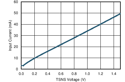
- 7.3.7 Thermal Foldback (TSNS)
- 7.3.8 Internal Regulator (VCC)
- 7.3.9 Error Amplifier (COMP)
- 7.3.10 Linear MOSFET Gate Drive (GDL)
- 7.3.11 EMI Filter
- 7.3.12 Thermal Shutdown
- 7.4 Device Functional Modes
- 8 Application and Implementation
- 9 Power Supply Recommendations
- 10Layout
- 11器件和文档支持
- 12机械封装和可订购信息
6 Specifications
6.1 Absolute Maximum Ratings
over operating free-air temperature range (unless otherwise noted) (1)| MIN | MAX | UNIT | ||
|---|---|---|---|---|
| Input voltage | VIN | –0.3 | 700 | V |
| Output voltage | VCC | –0.3 | 18 | V |
| GDL | –0.3 | 18 | ||
| MULT, VREF, ADIM, COMP, CPS, CDD, TSNS | –0.3 | 7.7 | ||
| DOV | –0.3 | 6 | ||
| Source current | CS | 1 | mA | |
| Sink current | CS | 1 | mA | |
| Operating junction temperature, TJ(2) | –40 | 150 | °C | |
(1) Stresses beyond those listed under Absolute Maximum Ratings may cause permanent damage to the device. These are stress ratings only, which do not imply functional operation of the device at these or any other conditions beyond those indicated under Recommended Operating Conditions. Exposure to absolute-maximum-rated conditions for extended periods may affect device reliability.
(2) Maximum junction temperature is internally limited by the device.
6.2 Handling Ratings
| MIN | MAX | UNIT | |||
|---|---|---|---|---|---|
| Tstg | Storage temperature range | –65 | 150 | °C | |
| V(ESD)(1) | Electrostatic discharge | Human body model (HBM), per ANSI/ESDA/JEDEC JS-001, all pins(2) | –1 | 1 | kV |
| Charged device model (CDM), per JEDEC specification JESD22-C101, all pins(3) | –250 | 250 | V | ||
(1) Electrostatic discharge (ESD) to measure device sensitivity and immunity to damage caused by assembly line electrostatic discharges into the device.
(2) Level listed above is the passing level per ANSI/ESDA/JEDEC JS-001. JEDEC document JEP155 states that 500V HBM allows safe manufacturing with a standard ESD control process. Terminals listed as 1000V may actually have higher performance.
(3) Level listed above is the passing level per EIA-JEDEC JESD22-C101. JEDEC document JEP157 states that 250V CDM allows safe manufacturing with a standard ESD control process. Terminals listed as 250V may actually have higher performance.
6.3 Recommended Operating Conditions
over operating free-air temperature range (unless otherwise noted)| MIN | NOM | MAX | UNIT | ||
|---|---|---|---|---|---|
| VIN | Input voltage | 9.5 | 450 | V | |
| VMULT | Multiplier peak input voltage | 3 | V | ||
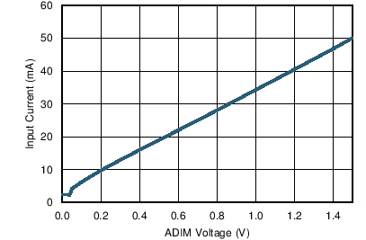
| VADIM | Analog dimming input voltage | 0 | 3 | V | |
| TJ | Operating junction temperature | -40 | 125 | °C | |
6.4 Thermal Information
| THERMAL METRIC(1) | TPS92410 | UNIT | |
|---|---|---|---|
| D (13) | |||
| RθJA | Junction-to-ambient thermal resistance | 84.8 | °C/W |
| RθJC(top) | Junction-to-case (top) thermal resistance | 39.8 | |
| RθJB | Junction-to-board thermal resistance | 39.5 | |
| ψJT | Junction-to-top characterization parameter | 8.9 | |
| ψJB | Junction-to-board characterization parameter | 39.0 | |
| RθJC(bot) | Junction-to-case (bottom) thermal resistance | N/A | |
(1) For more information about traditional and new thermal metrics, see the IC Package Thermal Metrics application report, SPRA953.
6.5 Electrical Characteristics
–40°C ≤ TJ ≤ 125°C, VVIN = 100 V, VADIM = VMULT = 1 V (unless otherwise noted)| PARAMETER | TEST CONDITIONS | MIN | TYP | MAX | UNIT | |
|---|---|---|---|---|---|---|
| SUPPLY VOLTAGE (VIN) | ||||||
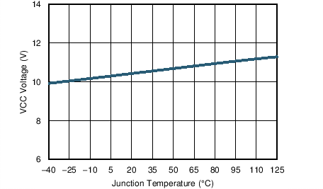
| VCC | Pre-regulator output voltage | 10.15 | V | |||
| VCCUVLO | Supply votlage undervoltage protection | Rising threshold, VVIN = VVCC | 8 | 8.3 | V | |
| Falling threshold, VVIN = VVCC | 5 | 5.85 | ||||
| Hysteresis | 2.15 | |||||
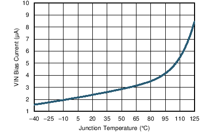
| IVIN | Input voltage bias current | VVCC = 12 V | 2.5 | 50 | μA | |
| IVCC | Supply bias current | 305 | 500 | μA | ||
| Supply standby current | VVIN = 0 V, VVCC = 7 V (UVLO) | 145 | ||||
| IVCCLIM | VCC supply current limit | VVCC = 7.5 V | 8 | 25 | mA | |
| Tplh(UVLO) | VCC supply glitch filter rising | VVCC stepped from 6.075 V to 110% of VCCUVLO,rising | 16.2 | μs | ||
| MULTIPLIER (MULT) | ||||||
| VMULT,LINEAR | Multiplier linear range | 0 | 3.5 | V | ||
| VCOMP,LINEAR | COMP pin linear range | 1.5 | 3.25 | V | ||
| RMULT | Input impedance | 500 | 580 | 700 | kΩ | |
| AMULT | Multiplier gain | VMULT = 1.5 V, VCOMP = 2.25 V, k = VMULT_OUT/[(VCOMP–1.5 V) × VMULT] |
0.95 | 1.43 | 1.85 | 1/V |
| VMULT,OFFSET | Multiplier output offset | VMULT = 0 V, VCOMP = 2.25 V | 13.7 | mV | ||
| MULTOUT,mx | Multiplier Output Clamp Voltage | VADIM = VTSNS = open; VCOMP = 4 V, VMULT = 3.5 V | 2.25 | 2.43 | 2.65 | V |
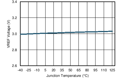
| VOLTAGE REFERENCE (VREF) | ||||||
| VVREF | Reference voltage | IVREF = 100 μA | 2.85 | 3 | 3.15 | V |
| VREFLINE | Line regulation | 8.5 V ≤ VVIN ≤ 100 V | 1% | |||
| VREFLOAD | Load regulation | 10 μA ≤ IREF ≤ 200 μA | 1% | |||
| TRANSCONDUCTANCE AMPLIFIER (ADIM, COMP) | ||||||
| ADIMLIM | ADIM operating voltage limit | 1.425 | 1.5 | 1.575 | V | |
| IADIM | Pull-up current | 0.5 | 1 | μA | ||
| ADIMSD | ADIM linear shutdown threshold | Falling | 18 | 40 | 70 | mV |
| ADIMSD,HYS | ADIM shutdown hysteresis | 20 | mV | |||
| gM | Transconductance | 43.3 | μS | |||
| VOFFSET | Input offset voltage | VADIM = 0.5 V | -20 | 20 | mV | |
| IOUT,SOURCE | Output source current | VCOMP = 2.25 V, VMULT = 0V, VADIM = VTSNS = 2 V |
65 | μA | ||
| IOUT,SINK | Output sink current | VCOMP = 2.25 V, VTSNS = 0 V | 75 | |||
| ISTART | VCOMP = 0 V, VADIM = 0 V | 485 | ||||
| DIMMER DETECT (MULT, CPS, CDD) | ||||||
| ICPS | Charge current for CPS pin | 6.7 | 10 | 13.3 | μA | |
| ICDD,c | Charge current for CDD pin | 5.7 | 10 | 13.3 | ||
| ICDD,d | Discharge current for CDD pin | 0.67 | 1 | 1.33 | ||
| Dv/Dt | Maximum detection threshold | VMULT stepped from 0 V to 1 V, minimum slew rate required | 1/100 | V/μs | ||
| VOFFSET | Detector offset voltage | 0.41 | V | |||
| VTH,CDD | CDD threshold | 1.5 | ||||
| VTH,CPS | CPS threshold | 1.5 | ||||
| RCSP | Pull down RDS(on) | 314 | Ω | |||
| DRAIN OVER-VOLTAGE (DOV) | ||||||
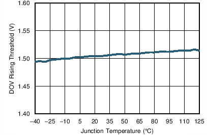
| VTH,DOV | Drain over-voltage threshold | 1.38 | 1.5 | 1.62 | V | |
| VHYS,DOV | Internal DOV hysteresis | 20 | mV | |||
| IHYS,DOV | Drain over-voltage source current | VDOV = 1.5 V, Device in over-voltage mode | 0.7 | 1 | 1.5 | μA |
| VREF,DOV | Linear CS reference during over-voltage | VDOV = 1.75 V | 0.1 | V | ||
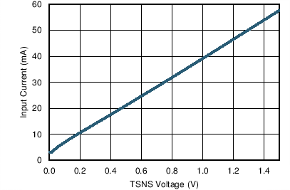
| THERMAL FOLDBACK (TSNS) | ||||||
| TSNSLIM | TSNS operating voltage limit | 1.425 | 1.5 | 1.575 | V | |
| VADIM = VTSNS = 1 V, Measure reference to the linear error amplifier | 2.1 | mV | ||||
| VTSNS = 0 V, Measure reference to the linear error amplifier | 3.6 | |||||
| ITSNS | Pull-up current | 0.5 | 1 | µA | ||
| LINEAR CURRENT SENSE (CS) | ||||||
| VCS(max) | CS voltage level (CC dimming mode) | 2.5 V = VADIM = VTSNS | 1.425 | 1.5 | 1.575 | V |
| VCS(max) | CS voltage level (PFC mode) | 2.5 V = VADIM = VTSNS | 1.125 | 1.291 | 1.425 | |
| VIO | Input offset voltage | VREF = 1 V | –17 | 2.57 | 17 | mV |
| VCMR– | Minimum input common mode range | 0 | V | |||
| GATE DRIVER (GDL) | ||||||
| VOH | High-level output voltage, GDL | ILOAD = –1 mA | 6.5 | 8.2 | V | |
| VOL | Low-level output voltage, GDL | ILOAD = 1 mA | 0.152 | 0.45 | ||
| IOUT(src) | Output source current | VGDL= 4 V | 2.5 | 8.1 | mA | |
| IOUT(snk) | Output sink current | VGDL= 4 V | 2.5 | 11.9 | ||
| THERMAL SHUTDOWN | ||||||
| TSD | Thermal shutdown | 175 | °C | |||
| Thermal shutdown hysteresis | 10 | |||||
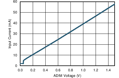
6.6 Typical Characteristics
Unless otherwise stated, –40°C ≤ TA = TJ ≤ +125°C. All characterization circuits are fully EMI compliant and phase dimmable.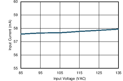
| 120VAC | 6.8 W Input | Top stack = 80 V |
| Middle stack = 40 V | Bottom stack= 20 V | VADIM = 1.5 V |
| 120VAC | 6.8 W Input | Top stack = 80 V |
| Middle stack = 40 V | Bottom stack= 20 V |
| 120VAC | 6.8 W Input | Top stack = 80 V |
| Middle stack = 40 V | Bottom stack= 20 V | VADIM = 1.5 V |
| VIN = 100 V | GDL Not Operating |
| 230 VAC | 11.2 W Input | Top stack = 160 V |
| Middle stack = 80 V | Bottom stack= 40 V | VADIM = 1.5 V |
| 230 VAC | 11.2 W Input | Top stack = 160 V |
| Middle stack = 80 V | Bottom stack= 40 V |
| 230 VAC | 11. W Input | Top stack = 160 V |
| Middle stack = 80 V | Bottom stack= 40 V | VADIM = 1.5 V |