ZHCSCM9 May 2014 TPS92410
PRODUCTION DATA.
- 1 特性
- 2 应用
- 3 说明
- 4 修订历史记录
- 5 Pin Configuration and Functions
- 6 Specifications
-
7 Detailed Description
- 7.1 Overview
- 7.2 Functional Block Diagram
- 7.3
Feature Description
- 7.3.1 Setting the Linear Regulator Current/Input Power (CS)
- 7.3.2 Over-Voltage Protecton (DOV)
- 7.3.3 Input Undervoltage Lockout (UVLO)
- 7.3.4 Reference Voltage (VREF)
- 7.3.5 Forward Phase Dimmer Detection (CPS, CDD)
- 7.3.6 Analog Dimming Input and Setting VCS (ADIM)
- 7.3.7 Thermal Foldback (TSNS)
- 7.3.8 Internal Regulator (VCC)
- 7.3.9 Error Amplifier (COMP)
- 7.3.10 Linear MOSFET Gate Drive (GDL)
- 7.3.11 EMI Filter
- 7.3.12 Thermal Shutdown
- 7.4 Device Functional Modes
- 8 Application and Implementation
- 9 Power Supply Recommendations
- 10Layout
- 11器件和文档支持
- 12机械封装和可订购信息
10 Layout
Proper layout is important in any regulator design. The TPS92410 is a linear regulator which simplifies layout compared to a switching regulator, however some consideration should be taken.
10.1 Layout Guidelines
Components between CPS, CDD, DOV, COMP, VREF, MULT, and VCC to ground (GND) should be placed directly next to the device as shown in Figure 18. The linear MOSFET as well as the GDL and CS traces should be placed as close the TPS92410 as possible as well.
10.2 Layout Example
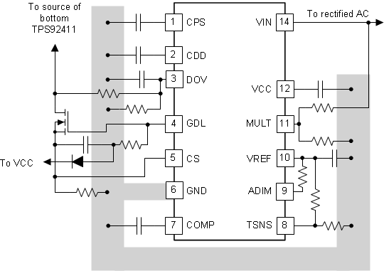 Figure 18. Recommended Component Placement