ZHCSCM9 May 2014 TPS92410
PRODUCTION DATA.
- 1 特性
- 2 应用
- 3 说明
- 4 修订历史记录
- 5 Pin Configuration and Functions
- 6 Specifications
-
7 Detailed Description
- 7.1 Overview
- 7.2 Functional Block Diagram
- 7.3
Feature Description
- 7.3.1 Setting the Linear Regulator Current/Input Power (CS)
- 7.3.2 Over-Voltage Protecton (DOV)
- 7.3.3 Input Undervoltage Lockout (UVLO)
- 7.3.4 Reference Voltage (VREF)
- 7.3.5 Forward Phase Dimmer Detection (CPS, CDD)
- 7.3.6 Analog Dimming Input and Setting VCS (ADIM)
- 7.3.7 Thermal Foldback (TSNS)
- 7.3.8 Internal Regulator (VCC)
- 7.3.9 Error Amplifier (COMP)
- 7.3.10 Linear MOSFET Gate Drive (GDL)
- 7.3.11 EMI Filter
- 7.3.12 Thermal Shutdown
- 7.4 Device Functional Modes
- 8 Application and Implementation
- 9 Power Supply Recommendations
- 10Layout
- 11器件和文档支持
- 12机械封装和可订购信息
7 Detailed Description
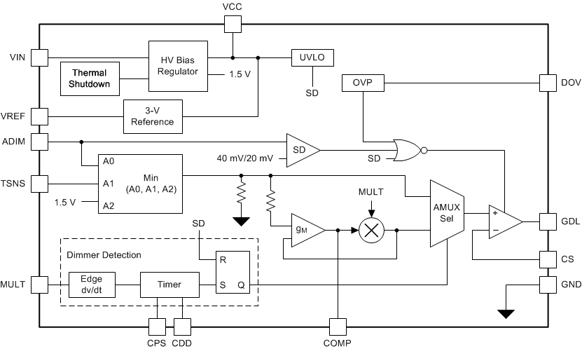
7.1 Overview
The TPS92410 device is a high-voltage linear regulator driver that can be used for offline LED drivers. It includes a feature that forces the regulator current to follow the rectified AC voltage to achieve high power-factor and low total harmonic distortion (THD). When the device detects multiple forward phase dimmer edges, the regulator current changes to a DC level to maintain a DC current draw to provide for a triac dimmer's hold current requirements. The TPS92410 device also includes linear MOSFET over-voltage protection to protect the MOSFET if the LEDs are shorted. It includes a thermal foldback feature to protect the entire circuit in the event it becomes overheated. Analog dimming capability allows light output to be controlled by a microcontroller or a 0 V to 10 V dimmer. The device also includes a precision voltage reference.
7.2 Functional Block Diagram
7.3 Feature Description
7.3.1 Setting the Linear Regulator Current/Input Power (CS)
The input power (PIN) can be set with a resistor from the CS pin to ground. Calculate the value of the RCS resistor using the following equation (see Figure 11):

where
- VIN(rms) is the nominal rms input voltage to the circuit
This sets the input power level due to the linear regulator for a standard application with VADIM and VTSNS greater than or equal to 1.5 V. If either pin is pulled below 1.5 V the input power scales accordingly to the ratio of VTSNS/ADIM/1.5 V. The actual input power of the circuit is higher due to variables such as VIN bias current, resistor, diode, and other losses. When using forward phase dimmers there can be a significant current spike through the MOSFET and RCS depending on the dv/dt of the dimmer edge. The magnitude and duration of this current spike should be measured in any application and a resistor should be chosen that is rated for the peak current required in any final design.
7.3.2 Over-Voltage Protecton (DOV)
The DOV pin can be used to set an over-voltage protection threshold for the external linear MOSFET. During normal operation DOV is not active, but in the event that the LEDs become shorted resulting in excessive voltage and power dissipation in the MOSFET over-voltage protection becomes active. During an over-voltage event, the CS pin regulation voltage defaults to 100 mV to reduce power dissipation in the MOSFET but still provide some light with the remaining LEDs. For this reason it is recommended to use a nominal value for CS for normal operation higher than 100 mV. A resistor divider to DOV between the MOSFET drain and system ground sets this over-voltage level as shown in Figure 11. During an over-voltage event the DOV pin sources 1 µA to provide some hysteresis. The level and hysteresis can be set using the following equations:


where
- VOVP is the desired maximum drain voltage
- RDRAIN is the resistor from DOV to the drain
- RGROUND is the resistor from DOV to system ground
Include a capacitor from the DOV pin to system ground to prevent the circuit from transitioning into over-voltage protection mode during the start-up sequence. A recommended value for the RGND resistor is 121 kΩ in parallel with a 4.7-µF capacitor for most applications. RDRAIN can then be calculated. To calculate the values of RGND and CGND for a particular application you need to set the time constant to be longer than it takes to charge up the highest voltage LED string capacitor to prevent a false trip of the over-voltage protection during start-up. This time constant and the resulting RC can be found using the following equations:


where
- dt is the time constant to charge the LED capacitor
- CUPPER is the highest voltage LED string capacitor
- VUPPER is the highest string voltage
- IUPPER is the highest voltage LED string current
Choose RGND to be in the 100 kΩ to 150 kΩ range and calculate CGND. Then RDRAIN can be calculated. Over-voltage protection should be adjusted for the minimum string voltages for analog dimming applications or simply disabled by connecting DOV to ground.
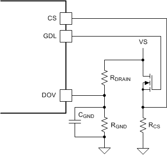 Figure 11. CS and DOV Over-voltage Connections
7.3.3 Input Undervoltage Lockout (UVLO)
The TPS92410 device includes input UVLO protection. This protection prevents the device from operating until a voltage on the VIN pin exceeds 8.0 V. The circuit has 2.15 V of hysteresis to prevent false triggering.
7.3.4 Reference Voltage (VREF)
The TPS92410 includes a 3-V reference feature which can be used to set the DC level on the ADIM pin. It can also source current for the TSNS divider for the thermal foldback circuitry using the TSNS pin. The VREF pin can supply a maximum current of approximately 3 mA but should be limited to less than 200 μA to minimize power dissipation. All current sourced from VREF is supplied by VIN so power dissipation can become significant when sourcing higher currents.
7.3.5 Forward Phase Dimmer Detection (CPS, CDD)
An edge-detect circuit senses when a forward phase dimmer is connected to the input. This detection feature allows the device to operate with a wide variety of dimmers that operate in either forward or reverse phase. The CCPS and CCDD capacitors assist in this function while preventing a false dimmer detect caused by line glitches and spikes in applications without a phase dimmer. Connect a 0.1-μF capacitor between CPS to GND and a 1-μF capacitor from CDD to GND for most applications to use this feature. This results in a time constant of 15 ms for CPS and 150 ms for CDD. If this feature is not required leave CPS open and ground CDD.
The dimmer detect function operates by applying a 10 µA charging current to both the CPS and CDD capacitors. If no edges are detected the CPS capacitor charges to a 1.5 V threshold at which point the CDD pin switches from sourcing 10 µA to sinking 1 µA. This prevents the CDD pin from charging to the 1.5-V threshold that switches the device to dimmer detect mode. When a forward phase dimmer is present the edge is detected at the MULT pin. Each time an edge is detected the CPS pin is discharged and then begins charging again. When enough consecutive edges are present to keep the CPS pin below 1.5 V for longer than the CDD time constant the CDD pin reaches 1.5 V and the device switches to dimmer detect mode. The current regulation level between constant current dimmer detect mode and standard PFC operation can be different depending on dimmer angle. A time constant too long can result in a mild light difference at turn-on due to a slightly different light level between PFC mode at turn-on and dimmer detect mode. A time constant too short could result in unintentionally switching to dimmer detect mode on noisy lines. The easiest way to implement a dimmer detect circuit is to use a CPS time constant just a bit longer than TPER, the period of half of the sine wave input voltage. But other time constants may be used if required. To change the time constants use the following equations:


7.3.6 Analog Dimming Input and Setting VCS (ADIM)
If a default CS voltage of lower than 1.291 V is required, it can be set using the ADIM pin. A resistor divider from the reference sets ADIM to any voltage lower than 1.5 V. During normal operation, the CS voltage is equal to 0.86 times the voltage applied to ADIM. The ADIM pin can also be used for analog dimming using a variable voltage between 40 mV and 1.5 V to dynamically change the CS voltage. If the device pulls the ADIM pin below 40 mV, the device pulls the linear MOSFET gate low to shut off the LEDs. Tie an unused ADIM pin to VREF with a 200-kΩ resistor. If a larger analog dimming range is required, use the TSNS pin for analog dimming because it does not disable the linear regulator when the voltage drops below 40 mV. The ADIM and TSNS pins function identically with the exception of the GDL disable threshold on the ADIM pin.
7.3.7 Thermal Foldback (TSNS)
The thermal foldback function of the TPS92410 device behaves similarly to the ADIM function. However, rather than using a resistor divider, a NTC thermistor connects TSNS to system ground. Calculate the temperature at which the circuit begins to reduce current by determining the temperature at which the the TSNS pin drops below 1.5 V (when the ADIM pin is 1.5 V or higher). With a valid external voltage on the ADIM pin (< 1.5 V), the current begins to reduce when the TSNS voltage drops lower than the ADIM voltage. As described in the Analog Dimming Input and Setting VCS (ADIM) section, the TSNS pin and the ADIM pin may be used interchangeably. If the TSNS pin is used for analog dimming, the ADIM pin may be used for thermal foldback.
7.3.8 Internal Regulator (VCC)
The VCC pin functions as the output of the internal supply for the device. Connect a 10-µF capacitor between the VCC pin and ground to keep VCC charged for phase dimming applications. For analog dimming or non-dimming applications a 4.7-µF capacitor is sufficient.
7.3.9 Error Amplifier (COMP)
The COMP pin functions as the output of the internal gM error amplifier. To ensure stability over all conditions, connect a 4.7-µF capacitor between the COMP pin and ground. The bandwidth of the PFC can be calculated using the following equation:

7.3.10 Linear MOSFET Gate Drive (GDL)
The GDL pin functions as the gate drive for the linear MOSFET that regulates current. Connect the GDL pin to the gate of the power MOSFET. To reduce EMI, connect a 10-Ω resistor in series with a 1-µF capacitor between the GDL pin and the CS pin with a diode connected between them that returns to the VCC pin as show in Figure 12. If phase dimming is not required, the diode can be omitted. Choose a linear MOSFET with a voltage rating of at least 250 V for a 120-VAC input application. Choose a linear MOSFET with a voltage rating of at least 400 V for a 230-VAC input application. The MOSFET voltage rating must take into account the MOV clamp voltage in protected applications as this may be higher than the MOSFET and damage may occur during a surge event. The Safe Operating Area (SOA) of the MOSFET must also be taken into account. During start-up the MOSFET experiences high voltages as the LED capacitors charge. This leads to high power dissipation during start-up that the MOSFET must withstand. Use with forward phase dimmers also causes a significant current spike in the MOSFET when the dimmer fires. The magnitude and duration of this current spike is dependent upon many factors and should be measured in any design to confirm the MOSFET is rated properly for long life operation. MOSFET parasitics should also be considered. A very large MOSFET with high parasitic capacitances can cause erroneous switching of the TPS92411 floating drivers.
7.3.11 EMI Filter
The input EMI filter requirements are specific to each design. A capacitor is needed for filtering and may also require an input resistor. For forward phase applications a snubber across the capacitor is likely to be required. The input resistor and snubber resistor need to have a pulse rating high enough for the particular application both during start-up and during forward phase dimming.
7.3.12 Thermal Shutdown
The TPS92410 device includes thermal shutdown protection. If the die temperature reaches approximately 175°C the device shuts down. When the die temperature cools to approximately 165°C, the device resumes normal operation.
7.4 Device Functional Modes
7.4.1 Multiplier Mode
When the MULT pin detects full rectified AC voltage, the CS voltage follows the rectified AC waveform around its regulation point. This behavior forces the current that is drawn from the line to follow the AC input voltage waveform. This action results in high power factor and low total harmonic distortion (THD). Line transients are rejected by the time constant that is initially set on the dimmer detect circuit to ensure dimmer detect mode is not engaged by random voltage spikes on the line.
7.4.2 Dimmer Detect Mode
When a forward phase dimmer is present there is a sharp edge presented to the MULT pin each cycle. This forces the dimmer detect circuit past its time constant and the device enters dimming mode. The CS voltage is then set at a DC level to prevent dimmer misfire