ZHCSCM9 May 2014 TPS92410
PRODUCTION DATA.
- 1 特性
- 2 应用
- 3 说明
- 4 修订历史记录
- 5 Pin Configuration and Functions
- 6 Specifications
-
7 Detailed Description
- 7.1 Overview
- 7.2 Functional Block Diagram
- 7.3
Feature Description
- 7.3.1 Setting the Linear Regulator Current/Input Power (CS)
- 7.3.2 Over-Voltage Protecton (DOV)
- 7.3.3 Input Undervoltage Lockout (UVLO)
- 7.3.4 Reference Voltage (VREF)
- 7.3.5 Forward Phase Dimmer Detection (CPS, CDD)
- 7.3.6 Analog Dimming Input and Setting VCS (ADIM)
- 7.3.7 Thermal Foldback (TSNS)
- 7.3.8 Internal Regulator (VCC)
- 7.3.9 Error Amplifier (COMP)
- 7.3.10 Linear MOSFET Gate Drive (GDL)
- 7.3.11 EMI Filter
- 7.3.12 Thermal Shutdown
- 7.4 Device Functional Modes
- 8 Application and Implementation
- 9 Power Supply Recommendations
- 10Layout
- 11器件和文档支持
- 12机械封装和可订购信息
5 Pin Configuration and Functions
SOIC HV
13 PIN
(TOP VIEW)
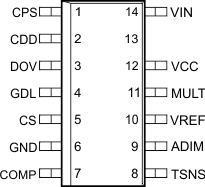
Pin Functions
| PIN | TYPE(1) | DESCRIPTION | |
|---|---|---|---|
| NAME | NO. | ||
| ADIM | 9 | I | Analog input used to set the reference of the linear controller. A 0-V to 1.5-V signal on ADIM sets the current sense reference level. |
| CDD | 2 | I/O | A capacitor to ground sets the time interval for dimmer detection. Tie to GND if no phase dimmer operation is required. |
| COMP | 7 | I/O | Compensation for control loop. Connect a capacitor from the COMP pin to ground. |
| CPS | 1 | I/O | A capacitor to ground sets the length of the CDD pin charge pulse. Leave open if no phase dimmer operation is required. |
| CS | 5 | I | Current sense input used for linear regulator. |
| DOV | 3 | I | Input to monitor linear MOSFET drain voltage. A resistor divider from the DOV pin to the drain connection of the MOSFET monitors MOSFET over-voltage. Add a capacitor to GND for filtering. |
| GDL | 4 | O | Gate drive for an external linear MOSFET. |
| GND | 6 | G | Chip ground return. |
| MULT | 11 | I | AC input to the multiplier. Tap a resistor divider off the rectified line to this pin. |
| TSNS | 8 | I | Thermal sense input. Connect to a resistor and NTC thermistor for thermal foldback. |
| VCC | 12 | I/O | Pre-regulated voltage. Connect a bypass capacitor to ground. |
| VIN | 14 | P | High voltage input. Provides power to the device. |
| VREF | 10 | O | 3-V voltage supply reference. Source used for TSNS input. |
(1) I = Input, O = Output, P = Supply, G = Ground