ZHCS831E march   2012  – may 2023 TPS7A16-Q1

PRODUCTION DATA  

  1.   1
  2. 特性
  3. 应用
  4. 说明
  5. Revision History
  6. Pin Configuration and Functions
  7. Specifications
    1. 6.1 Absolute Maximum Ratings
    2. 6.2 ESD Ratings
    3. 6.3 Recommended Operating Conditions
    4. 6.4 Thermal Information
    5. 6.5 Electrical Characteristics
    6. 6.6 Typical Characteristics
  8. Detailed Description
    1. 7.1 Overview
    2. 7.2 Functional Block Diagram
    3. 7.3 Feature Description
      1. 7.3.1 Enable (EN)
      2. 7.3.2 Regulated Output (VOUT)
      3. 7.3.3 PG Delay Timer (DELAY)
    4. 7.4 Device Functional Modes
      1. 7.4.1 Power-Good
      2. 7.4.2 Power-Good Delay and Delay Capacitor
  9. Application and Implementation
    1. 8.1 Application Information
    2. 8.2 Typical Applications
      1. 8.2.1 TPS7A1601-Q1 Circuit as an Adjustable Regulator
        1. 8.2.1.1 Design Requirements
        2. 8.2.1.2 Detailed Design Procedure
          1. 8.2.1.2.1 Adjustable Voltage Operation
          2. 8.2.1.2.2 Resistor Selection
          3. 8.2.1.2.3 Capacitor Recommendations
          4. 8.2.1.2.4 Input and Output Capacitor Requirements
          5. 8.2.1.2.5 Feed-Forward Capacitor (Only for Adjustable Version)
          6. 8.2.1.2.6 Transient Response
        3. 8.2.1.3 Application Curves
      2. 8.2.2 Automotive Applications
        1. 8.2.2.1 Design Requirements
        2. 8.2.2.2 Detailed Design Procedure
          1. 8.2.2.2.1 Device Recommendations
        3. 8.2.2.3 Application Curves
      3. 8.2.3 Multicell Battery Packs
        1. 8.2.3.1 Design Requirements
        2. 8.2.3.2 Detailed Design Procedure
        3. 8.2.3.3 Application Curves
      4. 8.2.4 Battery-Operated Power Tools
        1. 8.2.4.1 Design Requirements
        2. 8.2.4.2 Detailed Design Procedure
        3. 8.2.4.3 Application Curves
    3. 8.3 Power Supply Recommendations
    4. 8.4 Layout
      1. 8.4.1 Layout Guidelines
        1. 8.4.1.1 Additional Layout Considerations
        2. 8.4.1.2 Power Dissipation
        3. 8.4.1.3 Thermal Considerations
      2. 8.4.2 Layout Examples
  10. Device and Documentation Support
    1. 9.1 接收文档更新通知
    2. 9.2 支持资源
    3. 9.3 Trademarks
    4. 9.4 静电放电警告
    5. 9.5 术语表
  11. 10Mechanical, Packaging, and Orderable Information

封装选项

机械数据 (封装 | 引脚)
散热焊盘机械数据 (封装 | 引脚)
订购信息

Typical Characteristics

at TA = –40°C to +125°C, VIN = VOUT(NOM) + 0.5 V or VIN = 3 V (whichever is greater), VEN = VIN, IOUT = 10 μA, CIN = 1 μF, COUT = 2.2 μF, and FB tied to OUT (unless otherwise noted)
GUID-8AC955A3-5EAD-4252-82DE-57778D3761EF-low.png
 
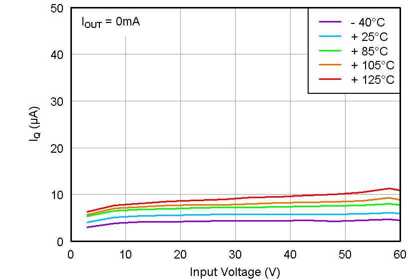
Figure 6-1 Quiescent Current vs Input Voltage
GUID-FD6B2D0E-4E31-424F-8E11-7B7D6365C741-low.png
 
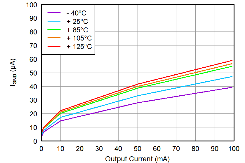
Figure 6-3 Quiescent Current vs Output Current
GUID-36F36FB8-397E-455B-AF59-920C2331D590-low.png
 
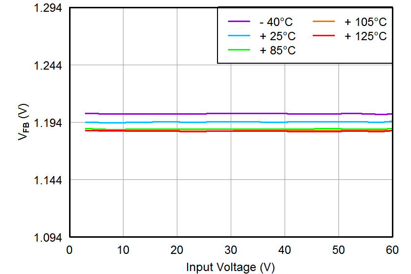
Figure 6-5 Feedback Voltage vs Input Voltage
GUID-21DAD91C-468C-40AB-A3DF-A43861A4857E-low.png
 
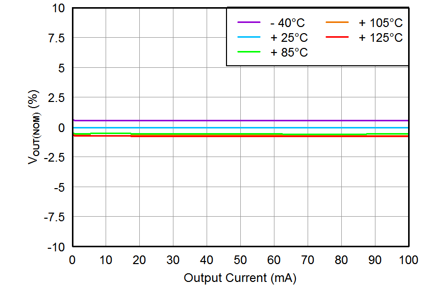
Figure 6-7 Load Regulation
GUID-1C043B09-3FA0-49E6-91A5-AFC7167536E4-low.png
 
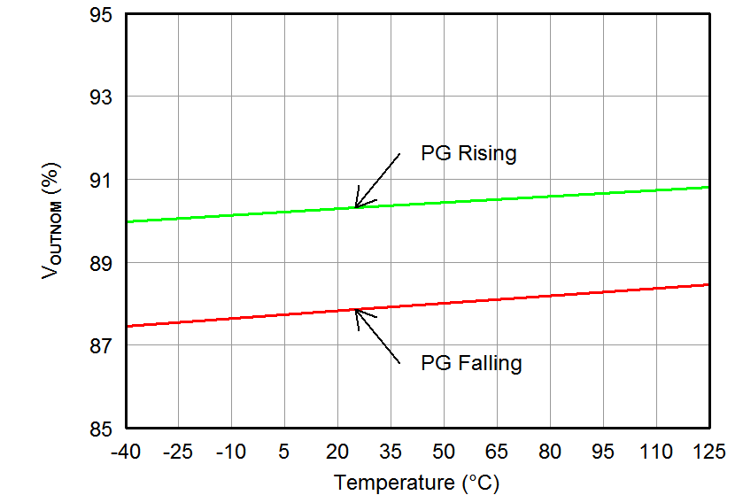
Figure 6-9 Power-Good Threshold Voltage vs Temperature
GUID-236DD8F9-AF02-47AE-8B56-D556FD50561D-low.png
 
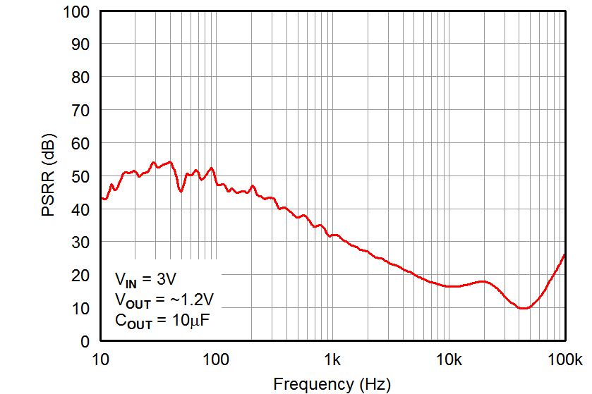
Figure 6-11 Power-Supply Rejection Ratio
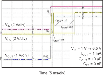
GUID-A7F3D95C-791F-43E2-85C4-72A052DE413E-low.gif
 
Figure 6-13 Power-Good Delay
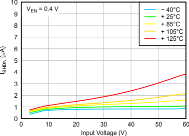
GUID-31E2CE36-E676-4E48-8D6B-C77E0632DF7D-low.gif
 
Figure 6-2 Shutdown Current vs Input Voltage
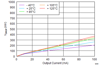
GUID-EEDAA380-A837-467A-BE14-8F0ED1A14E81-low.png
 
Figure 6-4 Dropout Voltage vs Output Current
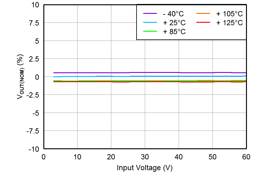
GUID-6B26E74E-5EE5-4364-9987-DAC6C4FA86A9-low.png
 
Figure 6-6 Line Regulation
GUID-BDCE4C8A-061A-4889-9590-9B9AA770E8BF-low.png
 
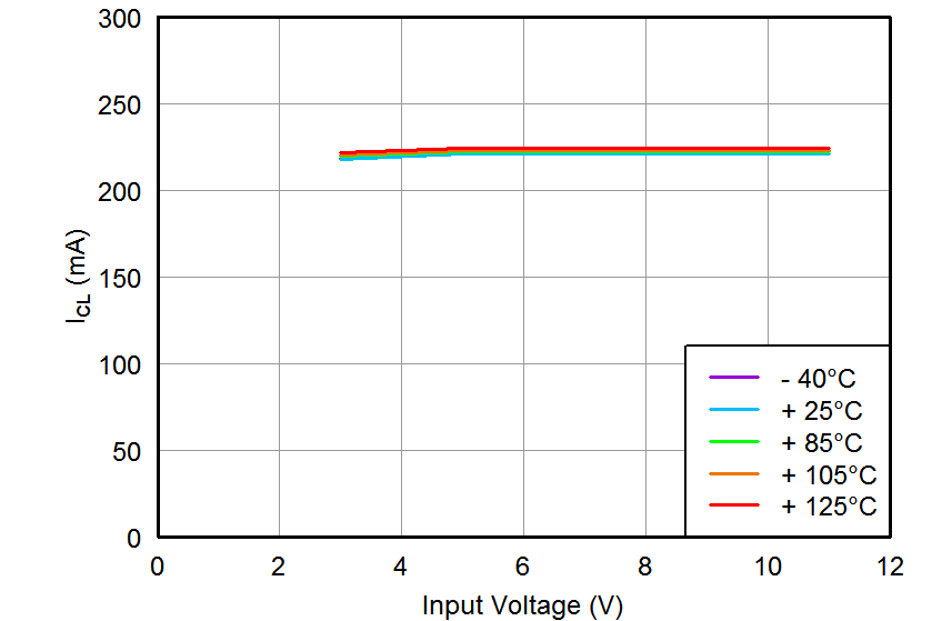
Figure 6-8 Current Limit vs Input Voltage
GUID-46DB07E2-AE90-4CAD-8AAF-744F358FC92B-low.png
 
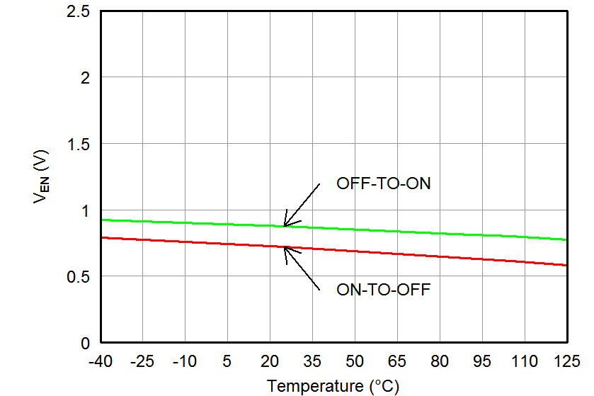
Figure 6-10 Enable Threshold Voltage vs Temperature
GUID-79850F06-38CD-477D-A422-520B6FED350B-low.png
 
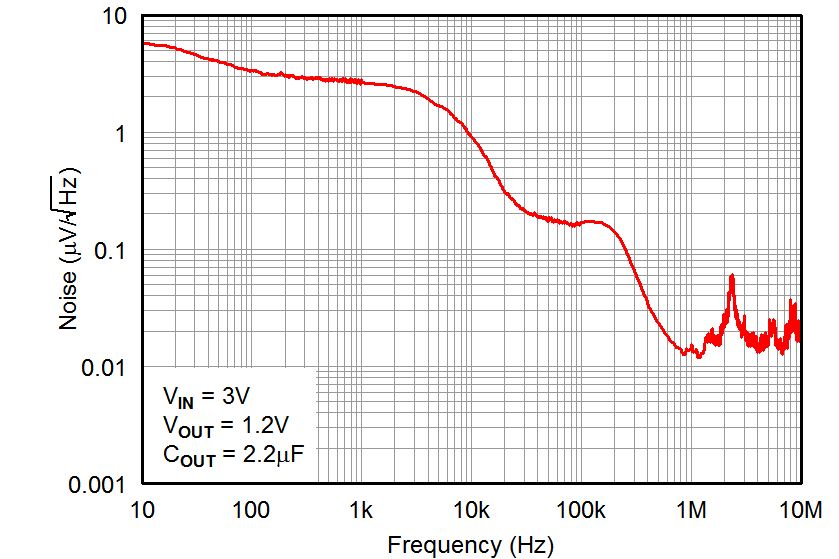
Figure 6-12 Output Spectral Noise Density