ZHCSIS2B september 2018 – december 2020 TPS7A11
PRODUCTION DATA
- 1
- 1 特性
- 2 应用
- 3 说明
- 4 Revision History
- 5 Pin Configuration and Functions
- 6 Specifications
- 7 Detailed Description
-
8 Application and Implementation
- 8.1
Application Information
- 8.1.1 Recommended Capacitor Types
- 8.1.2 Input and Output Capacitor Requirements
- 8.1.3 Load Transient Response
- 8.1.4 Dropout Voltage
- 8.1.5 Behavior During Transition From Dropout Into Regulation
- 8.1.6 Undervoltage Lockout Circuit Operation
- 8.1.7 Power Dissipation (PD)
- 8.1.8 Estimating Junction Temperature
- 8.1.9 Recommended Area for Continuous Operation
- 8.2 Typical Application
- 8.1
Application Information
- 9 Power Supply Recommendations
- 10Layout
- 11Device and Documentation Support
- Mechanical, Packaging, and Orderable Information
封装选项
机械数据 (封装 | 引脚)
散热焊盘机械数据 (封装 | 引脚)
- DRV|6
订购信息
7.3.2 Active Discharge
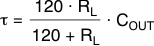
The active discharge option has an internal pulldown MOSFET that connects a 120-Ω resistor to ground when the device is disabled in order to actively discharge the output voltage. The active discharge circuit is activated by driving the enable pin to logic low to disable the device, or when the device is in thermal shutdown.
The discharge time after disabling the device depends on the output capacitance (COUT) and the load resistance (RL ) in parallel with the 120-Ω pulldown resistor. Equation 1 calculates this time:
Do not rely on the active discharge circuit for discharging a large amount of output capacitance after the input supply has collapsed because reverse current can flow from the output to the input. This reverse current flow can cause damage to the device. Limit reverse current to no more than 5% of the device-rated current.