ZHCSCV3A July 2013 – September 2014 TPS65631W
PRODUCTION DATA.
- 1 特性
- 2 应用范围
- 3 说明
- 4 简化电路原理图
- 5 修订历史记录
- 6 Pin Configuration and Functions
- 7 Specifications
-
8 Detailed Description
- 8.1 Overview
- 8.2 Functional Block Diagram
- 8.3 Feature Description
- 8.4 Device Functional Modes
- 8.5 Programming
- 9 Applications and Implementation
- 10Power Supply Recommendations
- 11Layout
- 12器件和文档支持
- 13机械封装和可订购信息
9 Applications and Implementation
NOTE
Information in the following applications sections is not part of the TI component specification, and TI does not warrant its accuracy or completeness. TI’s customers are responsible for determining suitability of components for their purposes. Customers should validate and test their design implementation to confirm system functionality.
9.1 Application Information
Figure 9 shows a typical application circuit suitable for supplying AMOLED displays in smartphone applications. The circuit is designed to operate from a single-cell Li-Ion battery and generates a positive output voltage VPOS of 4.6 V and a negative output voltage of –4 V. Both outputs are capable of supplying up to 300 mA of output current.
9.2 Typical Application
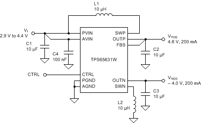 Figure 9. Typical Application Schematic
9.2.1 Design Requirements
For this design example, use the following input parameters.
Table 2. Design Parameters
| DESIGN PARAMETER | EXAMPLE |
|---|---|
| Input voltage range | 2.9 V to 4.5 V |
| Output voltage | VPOS = 4.6V, VNEG = –4 V |
9.2.2 Detailed Design Procedure
In order to maximize performance, the TPS65631W has been optimized for use with a relatively narrow range of component values, and customers are strongly recommended to use the application circuit shown in Figure 9 with the components listed in Table 3 and Table 4.
9.2.2.1 Inductor Selection
The boost converter and inverting buck-boost converter have been optimized for use with 10 µH inductors, and it is recommended that this value be used in all applications. Customers using other values of inductor are strongly recommended to characterize circuit performance on a case-by-case basis.
Table 3. Inductor Selection(1)
| PARAMETER | VALUE | MANUFACTURER | PART NUMBER |
|---|---|---|---|
| L1, L2 | 10 µH | Toko | DFE252012C-100M |
| ABCO | LPP252012-100M | ||
| Taiyo Yuden | MDKK2020T-100M |
9.2.2.2 Capacitor Selection
The recommended capacitor values are shown in Table 4. Applications using less than the recommended capacitance (e.g. to save PCB area) may experience increased voltage ripple. In general, the lower the output power, the lower the necessary capacitance.
Table 4. Capacitor Selection(1)
| PARAMETER | VALUE | MANUFACTURER | PART NUMBER |
|---|---|---|---|
| C1 | 2 × 10 µF | Murata | GRM21BR71A106KE51 |
| C2 | 10 µF | Murata | GRM21BR71A106KE51 |
| C3 | 2 × 10 µF | Murata | GRM21BR71A106KE51 |
| C4 | 100 nF | Murata | GRM21BR71E104KA01 |
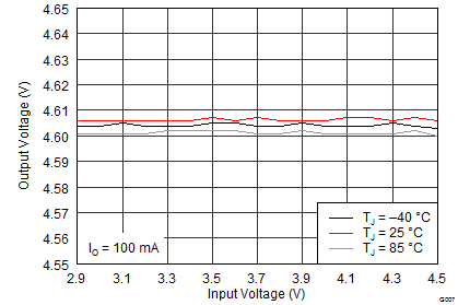
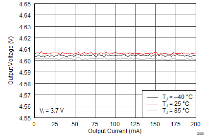
9.2.3 Application Curves
The performance shown in the following graphs was obtained using the circuit shown in Figure 9 and the external components shown in Table 3 and Table 4. The output voltage settings for these measurements were VPOS = 4.6 V and VNEG = –4 V.
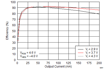
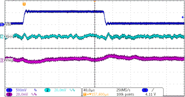
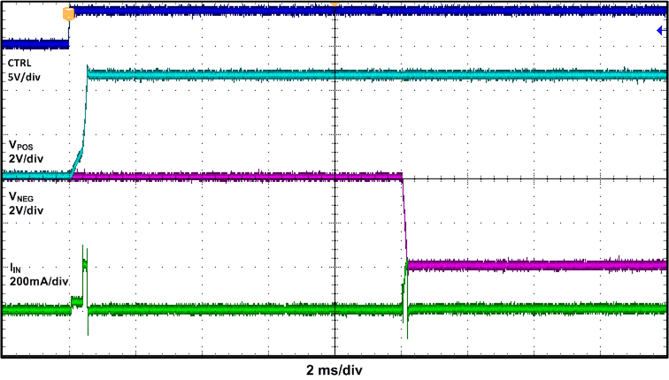 Figure 12. Start-Up Waveforms
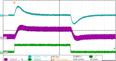
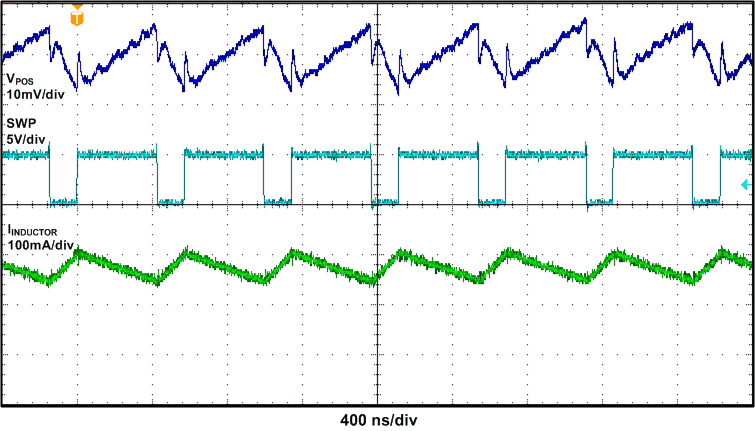 Figure 14. VPOS Switch Voltage, Inductor Current and Output Voltage Ripple (IO = 200 mA)
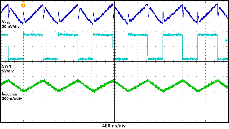
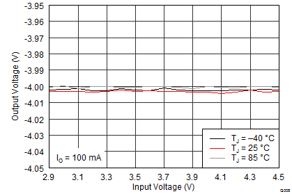
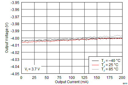
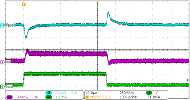
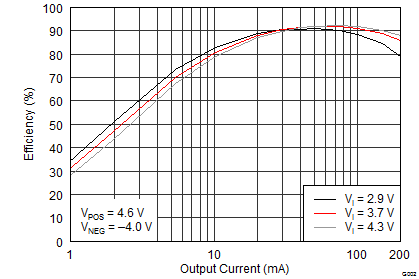
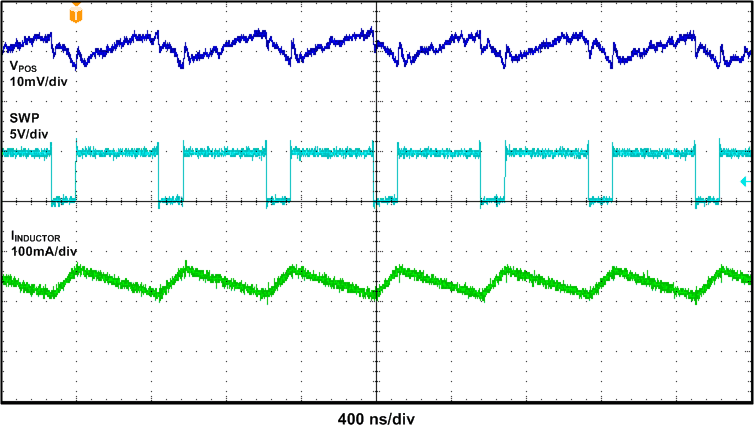 Figure 13. VPOS Switch Voltage, Inductor Current and Output Voltage Ripple (IO = 100 mA)
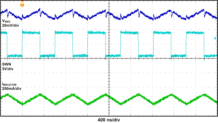 Figure 15. VNEG Switch Voltage, Inductor Current and Output Voltage Ripple (IO = 100 mA)