ZHCSCV3A July 2013 – September 2014 TPS65631W
PRODUCTION DATA.
- 1 特性
- 2 应用范围
- 3 说明
- 4 简化电路原理图
- 5 修订历史记录
- 6 Pin Configuration and Functions
- 7 Specifications
-
8 Detailed Description
- 8.1 Overview
- 8.2 Functional Block Diagram
- 8.3 Feature Description
- 8.4 Device Functional Modes
- 8.5 Programming
- 9 Applications and Implementation
- 10Power Supply Recommendations
- 11Layout
- 12器件和文档支持
- 13机械封装和可订购信息
7 Specifications
7.1 Absolute Maximum Ratings (1)
over operating free-air temperature range (unless otherwise noted) (1)| MIN | MAX | UNIT | ||
|---|---|---|---|---|
| Input voltage (2) | SWP, OUTP, FBS, PVIN, AVIN | –0.3 | 6 | V |
| OUTN | –0.3 | –6 | V | |
| SWN | –6 | 6 | V | |
| CTRL | –0.3 | 5.5 | V | |
| Operating junction temperature range, TJ | –40 | 150 | °C | |
(1) Stresses beyond those listed under Absolute Maximum Ratings may cause permanent damage to the device. These are stress ratings only, which do not imply functional operation of the device at these or any other conditions beyond those indicated under Recommended Operating Conditions. Exposure to absolute-maximum-rated conditions for extended periods may affect device reliability.
(2) With respect to AGND pin.
7.2 Handling Ratings
| MIN | MAX | UNIT | |||
|---|---|---|---|---|---|
| TSTG | Storage temperature range | –65 | 150 | °C | |
| VESD | Electrostatic discharge | Human body model (HBM), per ANSI/ESDA/JEDEC JS-001, all pins (1) | –2 | 2 | kV |
| Charged device model (CDM), per JEDEC specification JESD22-C101, all pins (2) | –500 | 500 | V | ||
| Machine model (MM) ESD stress voltage | –200 | 200 | V | ||
(1) JEDEC document JEP155 states that 500-V HBM allows safe manufacturing with a standard ESD control process.
(2) JEDEC document JEP157 states that 250-V CDM allows safe manufacturing with a standard ESD control process..
7.3 Recommended Operating Conditions
over operating free-air temperature range (unless otherwise noted)| PARAMETER | MIN | NOM | MAX | UNIT | ||
|---|---|---|---|---|---|---|
| VI | Input supply voltage range | 2.9 | 3.7 | 4.5 | V | |
| VO | Output voltage range | VPOS | 4.6 | V | ||
| VNEG | –4.4 | –4 | –1.4 | |||
| IO | Output current range | IPOS | 0 | 200 | mA | |
| INEG | 0 | 200 | ||||
| TA | Operating ambient temperature | –40 | 25 | 85 | °C | |
| TJ | Operating junction temperature | –40 | 85 | 125 | ||
7.4 Thermal Information
| THERMAL METRIC(1) | DSK | UNIT | |
|---|---|---|---|
| 10 PINS | |||
| RθJA | Junction-to-ambient thermal resistance | 47.1 | °C/W |
| RθJCtop | Junction-to-case (top) thermal resistance | 57.8 | |
| RθJB | Junction-to-board thermal resistance | 21.1 | |
| ψJT | Junction-to-top characterization parameter | 0.8 | |
| ψJB | Junction-to-board characterization parameter | 21.4 | |
| RθJCbot | Junction-to-case (bottom) thermal resistance | 4.3 | |
(1) For more information about traditional and new thermal metrics, see the IC Package Thermal Metrics application report, SPRA953.
7.5 Electrical Characteristics
VI = 3.7 V, V(CTRL) = 3.7 V, VPOS = 4.6 V, VNEG = –4.0 V, TJ = –40°C to 125°C, typical values are at TJ = 25°C (unless otherwise noted)| PARAMETER | TEST CONDITIONS | MIN | TYP | MAX | UNIT | |
|---|---|---|---|---|---|---|
| SUPPLY | ||||||
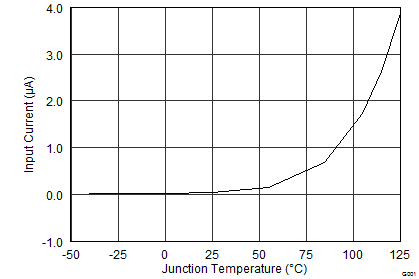
| II | Shutdown current into AVIN and PVIN | CTRL pin connected to ground. | 0.1 | µA | ||
| VUVLO | Undervoltage lockout threshold | VI rising. | 2.4 | V | ||
| VI falling. | 2.1 | |||||
| BOOST CONVERTER | ||||||
| VO | Output voltage | 4.6 | V | |||
| Output voltage tolerance | 25°C ≤ TJ ≤ 85°C, no load | –0.5% | 0.5% | |||
| –40°C ≤ TJ < 85°C, no load | –0.8% | 0.8% | ||||
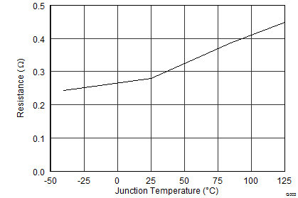
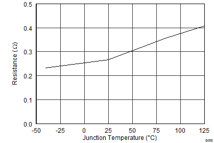
| rDS(ON) | Switch (low-side) on-resistance | I(SWP) = 200 mA | 200 | mΩ | ||
| Rectifier (high-side) on-resistance | I(SWP) = 200 mA | 350 | ||||
| Switching frequency | IO = 200 mA | 1.7 | MHz | |||
| Switch current limit | Inductor valley current | 0.8 | 1 | A | ||
| Short-circuit threshold voltage in operation | VO falling | 4.1 | V | |||
| Short-circuit detection time during operation | 3 | ms | ||||
| Output sense threshold voltage using OUTP | V(OUTP) - V(FBS) increasing | 300 | mV | |||
| Output sense threshold voltage using FBS | V(OUTP) - V(FBS) decreasing | 200 | mV | |||
| Input resistance of FBS | Between FBS pin and ground | 4 | MΩ | |||
| Discharge resistance | CTRL pin connected to ground, IO = 1 mA |
30 | Ω | |||
| Line regulation | IO = 200 mA | 0.002 | %/V | |||
| Load regulation | 0.01 | %/A | ||||
| INVERTING BUCK-BOOST CONVERTER | ||||||
| VO | Output voltage default | –4.0 | V | |||
| Output voltage range | –4.4 | –1.4 | ||||
| Output voltage tolerance | –0.05 | 0.05 | ||||
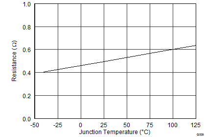
| rDS(ON) | Switch (high-side) on-resistance | I(SWN) = 200 mA | 200 | mΩ | ||
| Rectifier (low-side) on-resistance | I(SWN) = 200 mA | 300 | ||||
| Switching frequency | IO = 10 mA | 1.7 | MHz | |||
| Switch current limit | VI = 2.9 V | 1.5 | 2.2 | A | ||
| Short-circuit threshold voltage during operation | Voltage drop from nominal VO | 500 | mV | |||
| Short-circuit threshold voltage during start-up | 180 | 200 | 230 | |||
| tSCP | Short-circuit detection time during start-up | 10 | ms | |||
| Short-circuit detection time during operation | 3 | ms | ||||
| Discharge resistance | CTRL pin connected to ground, IO = 1 mA |
150 | Ω | |||
| Line regulation | IO = 200 mA | 0.006 | %/V | |||
| Load regulation | 0.31 | %/A | ||||
| CTRL | ||||||
| High-level threshold voltage | 1.2 | V | ||||
| Low-level threshold voltage | 0.4 | V | ||||
| Pull-down resistance | 150 | 400 | 860 | kΩ | ||
| OTHER | ||||||
| tINIT | Initialization time | 300 | 400 | µs | ||
| tOFF | Shut-down time | 30 | 80 | µs | ||
| tSTORE | Data storage time | 30 | 80 | µs | ||
| TSD | Thermal shutdown temperature | 145 | °C | |||
7.6 Timing Requirements
| MIN | TYP | MAX | UNIT | ||
|---|---|---|---|---|---|
| CTRL Interface | |||||
| tHIGH | High-level pulse duration | 2 | 10 | 25 | µs |
| tLOW | Low-level pulse duration | 2 | 10 | 25 | µs |
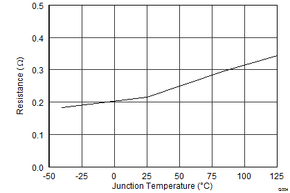
7.7 Typical Characteristics
At TA = 25°C, unless otherwise noted.