ZHCSCV3A July 2013 – September 2014 TPS65631W
PRODUCTION DATA.
- 1 特性
- 2 应用范围
- 3 说明
- 4 简化电路原理图
- 5 修订历史记录
- 6 Pin Configuration and Functions
- 7 Specifications
-
8 Detailed Description
- 8.1 Overview
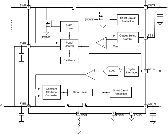
- 8.2 Functional Block Diagram
- 8.3 Feature Description
- 8.4 Device Functional Modes
- 8.5 Programming
- 9 Applications and Implementation
- 10Power Supply Recommendations
- 11Layout
- 12器件和文档支持
- 13机械封装和可订购信息
8 Detailed Description
8.1 Overview
The TPS65631W consists of a boost converter and an inverting buck boost converter. The VPOS output is fixed at 4.6 V and VNEG output is programmable via a digital interface in the range of -1.4 V ~ -4.4 V, the default is -4 V. The transition time of VNEG output is adjustable by the CT pin capacitor.
8.2 Functional Block Diagram
8.3 Feature Description
8.3.1 Boost Converter
The boost converter uses a fixed-frequency current-mode topology, and its output voltage (VPOS) is fixed at 4.6 V
For the highest output voltage accuracy, connect the output sense pin (FBS) directly to the positive pin of the output capacitor. If not used, the FBS pin can be left floating or connected to ground. If the FBS pin is not used, the boost converter senses its output voltage using the OUTP pin.
8.3.2 Inverting Buck-Boost Converter
The inverting buck-boost converter uses a constant-off-time peak-current mode topology. The converter's default output voltage (VNEG) is –4 V, but it can be programmed to any voltage in the range –1.4 V to –4.4 V (see Programming VNEG).
8.3.3 Soft-Start and Start-Up Sequence
The TPS65631W features a soft-start function to limit inrush current. When the device is enabled by a high-level signal applied to the CTRL pin, the boost converter starts switching with a reduced switch current limit. Ten milliseconds after the CTRL pin goes high, the inverting buck-boost converter starts with a default value of –4 V. A typical start-up sequence is shown in Figure 6.
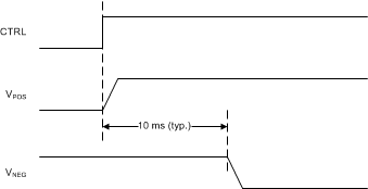 Figure 6. Typical Start-Up Sequence
8.3.4 Enable (CTRL)
The CTRL pin serves two functions. One is to enable and disable the device, and the other is to program the output voltage (VNEG) of the inverting buck-boost converter (see Programming VNEG). If the digital interface is not required, the CTRL pin can be used as a standard enable pin for the device, which will come up with its default value on VNEG of –4 V. When CTRL is pulled high, the device is enabled. The device is shut down with CTRL low.
8.3.5 Undervoltage Lockout
The TPS65631W features an undervoltage lockout function that disables the device when the input supply voltage is too low for normal operation.
8.3.6 Short Circuit Protection
The TPS65631W is protected against short-circuits of VPOS and VNEG to ground and to each other.
8.3.6.1 Short-Circuits During Normal Operation
During normal operation an error condition is detected if VPOS falls below 4.1 V for more than 3 ms or VNEG is pulled above the programmed nominal output by 500 mV for longer than 3 ms. In either case the device enters shutdown mode: the converters are disabled and their outputs are disconnected from the input. To resume normal operation either cycle the input supply voltage or toggle the CTRL pin low and then high again.
8.3.6.2 Short-Circuits During Start-Up
During start up an error condition is detected if:
- VPOS is not in regulation 10 ms after a high-level is applied to the CTRL pin.
- VNEG is higher than threshold level 10 ms after a high-level is applied to the CTRL pin.
- VNEG is not in regulation 20 ms after a high-level is applied to the CTRL pin.
To resume normal operation either cycle the input supply voltage or toggle the CTRL pin low and then high again.
8.3.7 Output Discharge During Shutdown
The TPS65631W actively discharges its outputs during shutdown. Figure 7 shows the output discharge control.
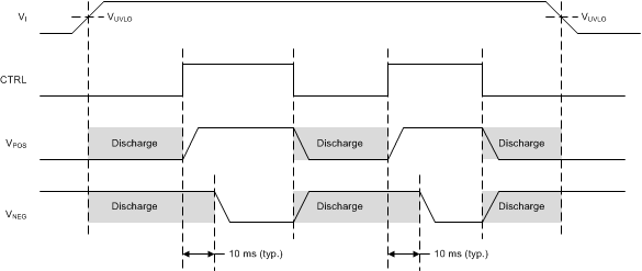 Figure 7. Active Discharge of VPOS and VNEG During Shutdown
8.3.8 Thermal Shutdown
The TPS65631W enters thermal shutdown mode if its junction temperature exceeds 145°C (typical). During thermal shutdown mode none of the device functions are available. To resume normal operation, either cycle the input supply voltage or toggle the CTRL pin low and then high again.
8.4 Device Functional Modes
8.4.1 Operation with VI < 2.9 V
The recommended minimum input supply voltage for full performance is 2.9 V. The device continues to operate with input supply voltages below 2.9 V; however, full performance is not guaranteed. The device does not operate with input supply voltages below the UVLO threshold.
8.4.2 Operation with VI ≈ VPOS (Diode Mode)
The TPS65631W features a "diode" mode that enables it to regulate its output voltage even when the input supply voltage is close to VPOS (that is, too high for normal boost operation). When operating in diode mode the converter's high-side switch stops switching and its body diode is used as the rectifier. Boost converter efficiency is reduced when operating in diode mode. At low output currents (≈2 mA and below), the boost converter automatically transitions from pulse-width modulation to pulse-skip mode. This ensures that VPOS stays in regulation but increases the output voltage ripple on VPOS.
8.4.3 Operation with CTRL
When a low-level signal is applied to the CTRL pin the device is disabled and switching is inhibited. When the input supply voltage is above the UVLO threshold and a high-level signal is applied to the CTRL pin the device is enabled and its start-up sequence begins.
8.5 Programming
8.5.1 Programming VNEG
The output voltage of the inverting buck-boost converter (VNEG) can be programmed using the CTRL pin. If output voltage programming is not required, the CTRL pin can be used as a standard enable pin (see Enable (CTRL)).
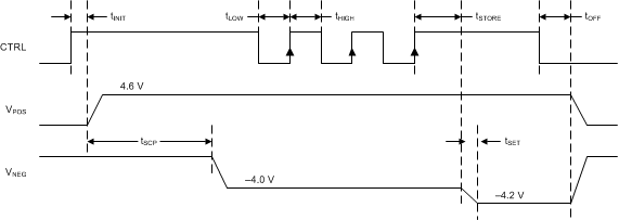 Figure 8. Programming VNEG Using the CTRL Pin
When the CTRL pin is pulled high, the inverting buck-boost converter starts up with its default voltage of –4V. The device now counts the rising edges applied to the CTRL pin and sets the output voltage (VNEG) according to Table 1. For the timing diagram shown in Figure 8, VNEG is programmed to –4.2 V, since three rising edges are detected.
The CTRL interface is designed to work with pulses whose duration is between 2 µs and 25 µs. Pulses shorter than 2 µs or longer than 25 µs are not ensured to be recognized.
Table 1. Programming Table for VNEG
| Number of Rising Edges | VNEG | Number of Rising Edges | VNEG |
|---|---|---|---|
| 0 / no pulses | –4 V | 16 | –2.9 V |
| 1 | –4.4 V | 17 | –2.8 V |
| 2 | –4.3 V | 18 | –2.7 V |
| 3 | –4.2 V | 19 | –2.6 V |
| 4 | –4.1 V | 20 | –2.5 V |
| 5 | –4.0 V | 21 | –2.4 V |
| 6 | –3.9 V | 22 | –2.3 V |
| 7 | –3.8 V | 23 | –2.2 V |
| 8 | –3.7 V | 24 | –2.1 V |
| 9 | –3.6 V | 25 | –2.0 V |
| 10 | –3.5 V | 26 | –1.9 V |
| 11 | –3.4 V | 27 | –1.8 V |
| 12 | –3.3 V | 28 | –1.7 V |
| 13 | –3.2 V | 29 | –1.6 V |
| 14 | –3.1 V | 30 | –1.5 V |
| 15 | –3.0 V | 31 | –1.4 V |