ZHCSCV3A July 2013 – September 2014 TPS65631W
PRODUCTION DATA.
- 1 特性
- 2 应用范围
- 3 说明
- 4 简化电路原理图
- 5 修订历史记录
- 6 Pin Configuration and Functions
- 7 Specifications
-
8 Detailed Description
- 8.1 Overview
- 8.2 Functional Block Diagram
- 8.3 Feature Description
- 8.4 Device Functional Modes
- 8.5 Programming
- 9 Applications and Implementation
- 10Power Supply Recommendations
- 11Layout
- 12器件和文档支持
- 13机械封装和可订购信息
6 Pin Configuration and Functions
SON (DSK) PACKAGE
10-PINS
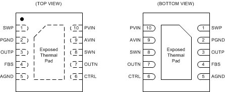
Pin Functions
| NAME | NO. | I/O | DESCRIPTION |
|---|---|---|---|
| AGND | 5 | — | Analog ground. |
| AVIN | 9 | — | Input supply voltage for internal analog circuits (both converters). |
| CTRL | 6 | I | Control pin. Combined device enable and inverting buck-boost converter output voltage programming pin. |
| FBS | 4 | I | Feedback sense pin of the boost converter output voltage. |
| PGND | 2 | — | Power ground of the boost converter. |
| PVIN | 12 | — | Input supply voltage pin for the inverting buck-boost converter. |
| SWN | 8 | O | Switch pin of the inverting buck-boost converter. |
| SWP | 1 | O | Switch pin of the boost converter. |
| OUTN | 7 | O | Rectifier pin of the inverting buck-boost converter. |
| OUTP | 3 | O | Rectifier pin of the boost converter. |
| Exposed Thermal Pad | 13 | — | Connect this pad to AGND and PGND. |