ZHCSCV3A July 2013 – September 2014 TPS65631W
PRODUCTION DATA.
- 1 特性
- 2 应用范围
- 3 说明
- 4 简化电路原理图
- 5 修订历史记录
- 6 Pin Configuration and Functions
- 7 Specifications
-
8 Detailed Description
- 8.1 Overview
- 8.2 Functional Block Diagram
- 8.3 Feature Description
- 8.4 Device Functional Modes
- 8.5 Programming
- 9 Applications and Implementation
- 10Power Supply Recommendations
- 11Layout
- 12器件和文档支持
- 13机械封装和可订购信息
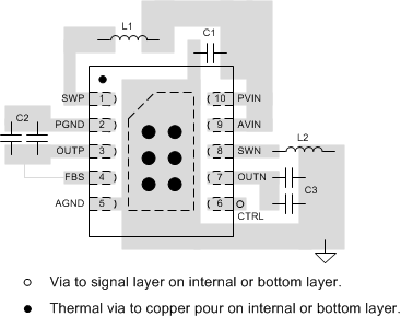
11 Layout
11.1 Layout Guidelines
No PCB layout is perfect and compromises are always necessary. However, following the basic principles listed below (in order of importance) should go a long way to achieving good performance:
- Route switching currents on the top layer using short, wide traces. Do not route these signals through vias, which have relatively high parasitic inductance and resistance.
- Use a copper pour on layer 2 as a ground plane and thermal spreader, and connect the thermal pad to it using a number of thermal vias.
- Place C1 as close as possible to pin 10.
- Place C2 as close as possible to pins 2 and 3.
- Place C3 as close as possible to pin 7.
- Place L1 as close as possible to pin 1.
- Place L2 as close as possible to pin 10.
- Use the thermal pad to join AGND and PGND.
- Connect the FBS pin directly to the positive pin of C2, that is, keep this connection separate from the connection between OUTP and C2.
Figure 24 illustrates how a PCB layout following the above principles may be realized in practice.