ZHCSAI3E May 2012 – March 2017 TPS65131-Q1
PRODUCTION DATA.
- 1 特性
- 2 应用范围
- 3 说明
- 4 修订历史记录
- 5 Pin Configuration and Functions
- 6 Specifications
- 7 Parameter Measurement Information
- 8 Detailed Description
-
9 Application and Implementation
- 9.1 Application Information
- 9.2
Typical Applications
- 9.2.1
TPS65131-Q1 With VPOS = 10.5 V, VNEG = -10 V
- 9.2.1.1 Design Requirements
- 9.2.1.2 Detailed Design Procedure
- 9.2.1.3 Analog Supply Input Filter
- 9.2.1.4 Thermal Information
- 9.2.1.5 Application Curves
- 9.2.2 TPS65131-Q1 With VPOS = 5.5 V, VNEG = -5 V
- 9.2.3 TPS65131-Q1 With VPOS = 15 V, VNEG = -15 V
- 9.2.1
TPS65131-Q1 With VPOS = 10.5 V, VNEG = -10 V
- 10Power Supply Recommendations
- 11Layout
- 12器件和文档支持
- 13机械、封装和可订购信息
封装选项
机械数据 (封装 | 引脚)
- RGE|24
散热焊盘机械数据 (封装 | 引脚)
- RGE|24
订购信息
6 Specifications
6.1 Absolute Maximum Ratings
over operating free-air temperature, unless otherwise noted (1)| VALUE | UNIT | |||
|---|---|---|---|---|
| MIN | MAX | |||
| Input voltage range at pins VIN, INN (2) | –0.3 | 6 | V | |
| Voltage at pin VPOS (2) | –0.3 | 17 | V | |
| Voltage at pin VNEG (2) | –17 | V(VIN) + 0.3 | V | |
| Voltage at pins ENN, ENP, FBP, FBN, CN, CP, PSP, PSN, BSW (2) | –0.3 | V(VIN) + 0.3 | V | |
| Input voltage at pin INP (2) | –0.3 | 17 | V | |
| Differential voltage between pins OUTN to INN (2) | –0.3 | 24 | V | |
| Thermal pad(2) | –0.3 | 0.3 | V | |
| TJ | Operating junction temperature | –40 | 150 | °C |
| Tstg | Storage temperature range | –65 | 150 | °C |
(1) Stresses beyond those listed under Absolute Maximum Ratings may cause permanent damage to the device. These are stress ratings only, which do not imply functional operation of the device at these or any other conditions beyond those indicated under Recommended Operating Conditions. Exposure to absolute-maximum-rated conditions for extended periods may affect device reliability.
(2) All voltage values are with respect to the network ground pin, unless otherwise noted.
6.2 ESD Ratings
| VALUE | UNIT | |||||
|---|---|---|---|---|---|---|
| V(ESD) | Electrostatic discharge | Human body model (HBM), per AEC Q100-002(1) | ±1000 | V | ||
| Charged device model (CDM), per AEC Q100-011 | ±750 | V | ||||
(1) AEC Q100-002 indicates HBM stressing is done in accordance with the ANSI/ESDA/JEDEC JS-001 specification.
6.3 Recommended Operating Conditions
over operating free-air temperature, unless otherwise noted| MIN | MAX | UNIT | ||
|---|---|---|---|---|
| VI , V(VIN), V(INN) | Application input voltage range, input voltage range at VIN and INN pins | 2.7 | 5.5 | V |
| VPOS | Adjustable output voltage range for the boost converter | VI + 0.5 | 15 | V |
| VNEG | Adjustable output voltage range for the inverting converter | –15 | –2 | V |
| V(ENN), V(ENP) | Enable signals voltage | 0 | 5.5 | V |
| V(PSN), V(PSP) | Power-save mode enable signals voltage | 0 | 5.5 | V |
| TA | Operating free-air temperature range(1) | –40 | 105 | °C |
| TJ | Operating junction temperature range | –40 | 125 | °C |
(1) In applications where high power dissipation and/or poor package thermal resistance is present, the maximum ambient temperature may require derating. See Thermal Information for details.
6.4 Thermal Information
| THERMAL METRIC(1) | TPS65131-Q1 | UNIT | |
|---|---|---|---|
| RGE PACKAGE | |||
| 24 PINS | |||
| RθJA | Junction-to-ambient thermal resistance | 34.1 | °C/W |
| RθJCtop | Junction-to-case (top) thermal resistance | 36.8 | °C/W |
| RθJB | Junction-to-board thermal resistance | 12.2 | °C/W |
| ψJT | Junction-to-top characterization parameter | 0.4 | °C/W |
| ψJB | Junction-to-board characterization parameter | 12.3 | °C/W |
| RθJCbot | Junction-to-case (bottom) thermal resistance | 2.8 | °C/W |
(1) For more information about traditional and new thermal metrics, see the Semiconductor and IC Package Thermal Metrics application report (SPRA953).
6.5 Electrical Characteristics
This specification applies over the full recommended input voltage range VI = 2.7 V to 5.5 V and over the temperature range TJ = –40°C to 125°C unless otherwise noted. Typical values apply for VI = 3.6 V and TJ = 25°C.6.6 Switching Characteristics
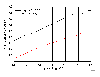
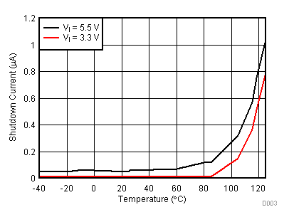
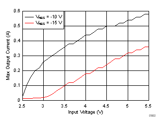
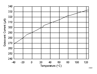
The specification applies over the full recommended input voltage range VI = 2.7 V to 5.5 V and over the temperature range TJ = –40 °C to 125°C unless otherwise noted. Typical values apply for VI = 3.6 V and TJ = 25°C.6.7 Typical Characteristics
At 25°C, unless otherwise noted.


| VI = 3.6 V |