ZHCSAI3E May 2012 – March 2017 TPS65131-Q1
PRODUCTION DATA.
- 1 特性
- 2 应用范围
- 3 说明
- 4 修订历史记录
- 5 Pin Configuration and Functions
- 6 Specifications
- 7 Parameter Measurement Information
- 8 Detailed Description
-
9 Application and Implementation
- 9.1 Application Information
- 9.2
Typical Applications
- 9.2.1
TPS65131-Q1 With VPOS = 10.5 V, VNEG = -10 V
- 9.2.1.1 Design Requirements
- 9.2.1.2 Detailed Design Procedure
- 9.2.1.3 Analog Supply Input Filter
- 9.2.1.4 Thermal Information
- 9.2.1.5 Application Curves
- 9.2.2 TPS65131-Q1 With VPOS = 5.5 V, VNEG = -5 V
- 9.2.3 TPS65131-Q1 With VPOS = 15 V, VNEG = -15 V
- 9.2.1
TPS65131-Q1 With VPOS = 10.5 V, VNEG = -10 V
- 10Power Supply Recommendations
- 11Layout
- 12器件和文档支持
- 13机械、封装和可订购信息
封装选项
机械数据 (封装 | 引脚)
- RGE|24
散热焊盘机械数据 (封装 | 引脚)
- RGE|24
订购信息
11 Layout
11.1 Layout Guidelines
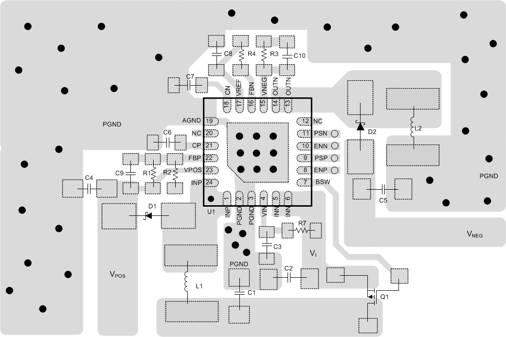
As for all switching power supplies, the layout is an important step in the design, especially at high peak currents and high switching frequencies. Improper layout might show the symptoms of poor line or load regulation, ground and output voltage shifts, stability issues, unsatisfying EMI behavior or worsened efficiency. Therefore, use wide and short traces for the main current paths and for the power ground tracks. The input capacitors (C1, C2, C3), output capacitors (C4, C5), the inductors (L1, L2), and the rectifying diodes (D1, D2) should be placed as close as possible to the IC to keep parasitic inductances low. Use a wide PGND plane. Connect the analog ground pin (AGND) to the PGND plane. Further, connect the PGND plane with the exposed thermal pad. Place the feedback dividers as close as possible to the control pin (boost converter) or the VREF pin (inverting converter) of the IC.
Figure 42 provides an layout example which is recommended to be followed.
11.2 Layout Example
 Figure 42. TPS65131-Q1 Layout Recommendation