ZHCSKR9A January   2020  – March 2020 TPS59603-Q1

PRODUCTION DATA.  

  1. 特性
  2. 应用
  3. 说明
    1.     Device Images
      1.      简化应用
  4. 修订历史记录
  5. Pin Configuration and Functions
    1.     Pin Functions
  6. Specifications
    1. 6.1 Absolute Maximum Ratings
    2. 6.2 ESD Ratings
    3. 6.3 Recommended Operating Conditions
    4. 6.4 Thermal Information
    5. 6.5 Electrical Characteristics
    6. 6.6 Typical Characteristics
  7. Detailed Description
    1. 7.1 Overview
    2. 7.2 Functional Block Diagram
    3. 7.3 Feature Description
      1. 7.3.1 UVLO Protection
      2. 7.3.2 PWM Pin
      3. 7.3.3 SKIP Pin
        1. 7.3.3.1 Zero Crossing (ZX) Operation
      4. 7.3.4 Adaptive Dead-Time Control and Shoot-Through Protection
      5. 7.3.5 Integrated Boost-Switch
    4. 7.4 Device Functional Modes
  8. Power Supply Recommendations
  9. Layout
    1. 9.1 Layout Guidelines
    2. 9.2 Layout Recommendation
  10. 10器件和文档支持
    1. 10.1 器件支持
      1. 10.1.1 开发支持
    2. 10.2 文档支持
      1. 10.2.1 相关文档
    3. 10.3 社区资源
    4. 10.4 商标
    5. 10.5 静电放电警告
    6. 10.6 Glossary
  11. 11机械、封装和可订购信息

封装选项

机械数据 (封装 | 引脚)
散热焊盘机械数据 (封装 | 引脚)
订购信息

UVLO Protection

The UVLO comparator evaluates the VDD voltage level. As VVDD rises, both DRVH and DRVL hold actively low at all times until VVDD reaches the higher UVLO threshold (VUVLO_H). Then, the driver becomes operational and responds to PWM and SKIP commands. If VDD falls below the lower UVLO threshold (VUVLO_L = VUVLO_H – Hysteresis), the device disables the driver and drives the outputs of DRVH and DRVL actively low. Figure 13 shows this function.

CAUTION

Do not start the driver in the very low power mode (SKIP = Tri-state).
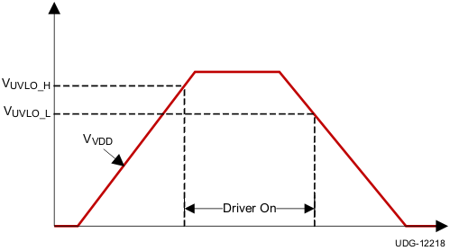
TPS59603-Q1 v12218_lusba6.gifFigure 13. UVLO Operation