ZHCSGO0A June 2017 – February 2024 TPS549B22
PRODUCTION DATA
- 1
- 1 特性
- 2 应用
- 3 说明
- 4 Pin Configuration and Functions
- 5 Specifications
-
6 Detailed Description
- 6.1 Overview
- 6.2 Functional Block Diagram
- 6.3 Feature Description
- 6.4 Device Functional Modes
- 6.5 Programming
-
7 Register Maps
- 7.1 OPERATION Register (address = 1h)
- 7.2 ON_OFF_CONFIG Register (address = 2h)
- 7.3 CLEAR FAULTS (address = 3h)
- 7.4 WRITE PROTECT (address = 10h)
- 7.5 STORE_DEFAULT_ALL (address = 11h)
- 7.6 RESTORE_DEFAULT_ALL (address = 12h)
- 7.7 CAPABILITY (address = 19h)
- 7.8 VOUT_MODE (address = 20h)
- 7.9 VOUT_COMMAND (address = 21h)
- 7.10 VOUT_MARGIN_HIGH (address = 25h) ®
- 7.11 VOUT_MARGIN_LOW (address = 26h)
- 7.12 STATUS_BYTE (address = 78h)
- 7.13 STATUS_WORD (High Byte) (address = 79h)
- 7.14 STATUS_VOUT (address = 7Ah)
- 7.15 STATUS_IOUT (address = 7Bh)
- 7.16 STATUS_CML (address = 7Eh)
- 7.17 MFR_SPECIFIC_00 (address = D0h)
- 7.18 MFR_SPECIFIC_01 (address = D1h)
- 7.19 MFR_SPECIFIC_02 (address = D2h)
- 7.20 MFR_SPECIFIC_03 (address = D3h)
- 7.21 MFR_SPECIFIC_04 (address = D4h)
- 7.22 MFR_SPECIFIC_06 (address = D6h)
- 7.23 MFR_SPECIFIC_07 (address = D7h)
- 7.24 MFR_SPECIFIC_44 (address = FCh)
-
8 Application and Implementation
- 8.1 Application Information
- 8.2
Typical Applications
- 8.2.1 TPS549B22 1.5-V to 18-V Input, 1-V Output, 25-A Converter
- 8.2.2 Design Requirements
- 8.2.3
Detailed Design Procedure
- 8.2.3.1 Custom Design With WEBENCH® Tools
- 8.2.3.2 Switching Frequency Selection
- 8.2.3.3 Inductor Selection
- 8.2.3.4 Output Capacitor Selection
- 8.2.3.5 Input Capacitor Selection
- 8.2.3.6 Bootstrap Capacitor Selection
- 8.2.3.7 BP Pin
- 8.2.3.8 R-C Snubber and VIN Pin High-Frequency Bypass
- 8.2.3.9 Optimize Reference Voltage (VSEL)
- 8.2.3.10 MODE Pin Selection
- 8.2.3.11 ADDR Pin Selection
- 8.2.3.12 Overcurrent Limit Design
- 8.2.4 Application Curves
- 8.3 Power Supply Recommendations
- 8.4 Layout
- 9 Device and Documentation Support
- 10Revision History
- 11Mechanical, Packaging, and Orderable Information
封装选项
请参考 PDF 数据表获取器件具体的封装图。
机械数据 (封装 | 引脚)
- RVF|40
散热焊盘机械数据 (封装 | 引脚)
- RVF|40
订购信息
8.2.3.4.1 Minimum Output Capacitance to Make Sure of Stability
To prevent sub-harmonic multiple pulsing behavior, TPS549B22 application designs must strictly follow the small signal stability considerations described in Equation 7.
Equation 7. 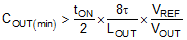
where
- COUT(min) is the minimum output capacitance needed to meet the stability requirement of the design
- tON is the on-time information based on the switching frequency and duty cycle (in this design, 128 ns)
- τ is the ramp compensation time constant of the design based on the switching frequency and duty cycle, (in this design, 25.9 µs, refer to Table 8-2)
- LOUT is the output inductance (in the design, 0.33 µH)
- VREF is the user-selected reference voltage level (in this design, 1 V)
- VOUT is the output voltage (in this design, 1 V)
The minimum output capacitance calculated from Equation 7 is 40 µF. The stability is ensured when the amount of the output capacitance is 40 µF or greater. And when all MLCCs (multi-layer ceramic capacitors) are used, both DC- and AC-derating effects must be considered to make sure that the minimum output capacitance requirement is met with sufficient margin.