ZHCSGO0A June 2017 – February 2024 TPS549B22
PRODUCTION DATA
- 1
- 1 特性
- 2 应用
- 3 说明
- 4 Pin Configuration and Functions
- 5 Specifications
-
6 Detailed Description
- 6.1 Overview
- 6.2 Functional Block Diagram
- 6.3 Feature Description
- 6.4 Device Functional Modes
- 6.5 Programming
-
7 Register Maps
- 7.1 OPERATION Register (address = 1h)
- 7.2 ON_OFF_CONFIG Register (address = 2h)
- 7.3 CLEAR FAULTS (address = 3h)
- 7.4 WRITE PROTECT (address = 10h)
- 7.5 STORE_DEFAULT_ALL (address = 11h)
- 7.6 RESTORE_DEFAULT_ALL (address = 12h)
- 7.7 CAPABILITY (address = 19h)
- 7.8 VOUT_MODE (address = 20h)
- 7.9 VOUT_COMMAND (address = 21h)
- 7.10 VOUT_MARGIN_HIGH (address = 25h) ®
- 7.11 VOUT_MARGIN_LOW (address = 26h)
- 7.12 STATUS_BYTE (address = 78h)
- 7.13 STATUS_WORD (High Byte) (address = 79h)
- 7.14 STATUS_VOUT (address = 7Ah)
- 7.15 STATUS_IOUT (address = 7Bh)
- 7.16 STATUS_CML (address = 7Eh)
- 7.17 MFR_SPECIFIC_00 (address = D0h)
- 7.18 MFR_SPECIFIC_01 (address = D1h)
- 7.19 MFR_SPECIFIC_02 (address = D2h)
- 7.20 MFR_SPECIFIC_03 (address = D3h)
- 7.21 MFR_SPECIFIC_04 (address = D4h)
- 7.22 MFR_SPECIFIC_06 (address = D6h)
- 7.23 MFR_SPECIFIC_07 (address = D7h)
- 7.24 MFR_SPECIFIC_44 (address = FCh)
-
8 Application and Implementation
- 8.1 Application Information
- 8.2
Typical Applications
- 8.2.1 TPS549B22 1.5-V to 18-V Input, 1-V Output, 25-A Converter
- 8.2.2 Design Requirements
- 8.2.3
Detailed Design Procedure
- 8.2.3.1 Custom Design With WEBENCH® Tools
- 8.2.3.2 Switching Frequency Selection
- 8.2.3.3 Inductor Selection
- 8.2.3.4 Output Capacitor Selection
- 8.2.3.5 Input Capacitor Selection
- 8.2.3.6 Bootstrap Capacitor Selection
- 8.2.3.7 BP Pin
- 8.2.3.8 R-C Snubber and VIN Pin High-Frequency Bypass
- 8.2.3.9 Optimize Reference Voltage (VSEL)
- 8.2.3.10 MODE Pin Selection
- 8.2.3.11 ADDR Pin Selection
- 8.2.3.12 Overcurrent Limit Design
- 8.2.4 Application Curves
- 8.3 Power Supply Recommendations
- 8.4 Layout
- 9 Device and Documentation Support
- 10Revision History
- 11Mechanical, Packaging, and Orderable Information
封装选项
请参考 PDF 数据表获取器件具体的封装图。
机械数据 (封装 | 引脚)
- RVF|40
散热焊盘机械数据 (封装 | 引脚)
- RVF|40
订购信息
8.2.3.5 Input Capacitor Selection
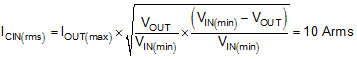
The TPS549B22 devices require a high-quality, ceramic, type X5R or X7R, input decoupling capacitor with a value of at least 1 μF of effective capacitance on the VDD pin, relative to AGND. The power stage input decoupling capacitance (effective capacitance at the PVIN and PGND pins) must be sufficient to supply the high switching currents demanded when the high-side MOSFET switches on, while providing minimal input voltage ripple as a result. This effective capacitance includes any DC bias effects. The voltage rating of the input capacitor must be greater than the maximum input voltage. The capacitor must also have a ripple current rating greater than the maximum input current ripple to the device during full load. The input ripple current can be calculated using Equation 12.
The minimum input capacitance and ESR values for a given input voltage ripple specification, VIN(ripple), are shown in Equation 13 and Equation 14. The input ripple is composed of a capacitive portion, VRIPPLE(cap), and a resistive portion, VRIPPLE(esr).
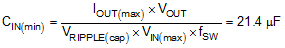
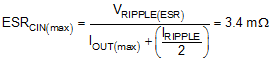
The value of a ceramic capacitor varies significantly over temperature and the amount of DC bias applied to the capacitor. The capacitance variations due to temperature can be minimized by selecting a dielectric material that is stable over temperature. X5R and X7R ceramic dielectrics are usually selected for power regulator capacitors because they have a high capacitance to volume ratio and are fairly stable over temperature. The input capacitor must also be selected with the DC bias taken into account. For this example design, a ceramic capacitor with at least a 25-V voltage rating is required to support the maximum input voltage. For this design, allow 0.1-V input ripple for VRIPPLE(cap), and 0.1-V input ripple for VRIPPLE(esr). Using Equation 13 and Equation 14, the minimum input capacitance for this design is 21.4 µF, and the maximum ESR is 3.4 mΩ. For this example, four 22-μF, 25-V ceramic capacitors and one additional 100-μF, 25-V low-ESR polymer capacitors in parallel were selected for the power stage.