ZHCSGV1C June 2017 – March 2018 TPS25740B
PRODUCTION DATA.
- 1 特性
- 2 应用
- 3 说明
- 4 修订历史记录
- 5 Device Comparison Table
- 6 Pin Configuration and Functions
- 7 Specifications
-
8 Detailed Description
- 8.1 Overview
- 8.2 Functional Block Diagram
- 8.3
Feature Description
- 8.3.1 ENSRC
- 8.3.2 USB Type-C CC Logic (CC1, CC2)
- 8.3.3 USB PD BMC Transmission (CC1, CC2, VTX)
- 8.3.4 USB PD BMC Reception (CC1, CC2)
- 8.3.5 Discharging (DSCG, VPWR)
- 8.3.6 Configuring Voltage Capabilities (HIPWR)
- 8.3.7 Configuring Power Capabilities (PSEL, PCTRL, HIPWR)
- 8.3.8 Gate Driver (GDNG, GDNS)
- 8.3.9 Fault Monitoring and Protection
- 8.3.10 Voltage Control (CTL1, CTL2,CTL3)
- 8.3.11 Sink Attachment Indicator (DVDD)
- 8.3.12 Power Supplies (VAUX, VDD, VPWR, DVDD)
- 8.3.13 Grounds (AGND, GND)
- 8.3.14 Output Power Supply (DVDD)
- 8.4 Device Functional Modes
-
9 Application and Implementation
- 9.1
Application Information
- 9.1.1 System-Level ESD Protection
- 9.1.2 Using ENSRC to Enable the Power Supply upon Sink Attachment
- 9.1.3 Use of GD Internal Clamp
- 9.1.4 Resistor Divider on GD for Programmable Start Up
- 9.1.5 Selection of the CTL1, CTL2, and CTL3 Resistors (R(FBL1), R(FBL2), and R(FBL3))
- 9.1.6 Voltage Transition Requirements
- 9.1.7 VBUS Slew Control using GDNG C(SLEW)
- 9.1.8 Tuning OCP using RF and CF
- 9.2 Typical Applications
- 9.3 System Examples
- 9.1
Application Information
- 10Power Supply Recommendations
- 11Layout
- 12器件和文档支持
- 13机械、封装和可订购信息
9.3.1 D/C Power Source (Power Hub)
In this system design example, the P(SEL) is configured such that P(SEL) = 93 W, so 5 V, 9 V, and 15 V are offered at a maximum of 5 A, while 20 V is offered at a maximum of 4.64 A. The over-current protection (OCP) trip point is set just above 5 A.
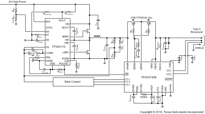
 Figure 67. Power Hub Concept (Provider only)
 This power hub circuit takes a 24 V input and produces a regulated output voltage. The over-current protection feature in the TPS25740B is not used; the ISNS and VBUS pins are connected directly. Instead R(ILIM) is chosen to set the current limit of the TPS40170 synchronous PWM buck controller. If the current limit trips, the GD pin of the TPS25740B is pulled low by the PGOOD pin of the TPS40170, which causes the power-path switch to be opened. Other fault conditions may also pull PGOOD low, but the slew rate of the voltage transition should be controlled as in one of the examples given above (Figure 44, Figure 45, or Figure 47).
VDD on the TPS25740B is grounded, if there is a suitable power supply available in the system the TPS25740B operates more efficiently if it is connected to VDD since V(VPWR) > V(VDD). See Figure 70 for an example.