ZHCSGV1C June 2017 – March 2018 TPS25740B
PRODUCTION DATA.
- 1 特性
- 2 应用
- 3 说明
- 4 修订历史记录
- 5 Device Comparison Table
- 6 Pin Configuration and Functions
- 7 Specifications
-
8 Detailed Description
- 8.1 Overview
- 8.2 Functional Block Diagram
- 8.3
Feature Description
- 8.3.1 ENSRC
- 8.3.2 USB Type-C CC Logic (CC1, CC2)
- 8.3.3 USB PD BMC Transmission (CC1, CC2, VTX)
- 8.3.4 USB PD BMC Reception (CC1, CC2)
- 8.3.5 Discharging (DSCG, VPWR)
- 8.3.6 Configuring Voltage Capabilities (HIPWR)
- 8.3.7 Configuring Power Capabilities (PSEL, PCTRL, HIPWR)
- 8.3.8 Gate Driver (GDNG, GDNS)
- 8.3.9 Fault Monitoring and Protection
- 8.3.10 Voltage Control (CTL1, CTL2,CTL3)
- 8.3.11 Sink Attachment Indicator (DVDD)
- 8.3.12 Power Supplies (VAUX, VDD, VPWR, DVDD)
- 8.3.13 Grounds (AGND, GND)
- 8.3.14 Output Power Supply (DVDD)
- 8.4 Device Functional Modes
-
9 Application and Implementation
- 9.1
Application Information
- 9.1.1 System-Level ESD Protection
- 9.1.2 Using ENSRC to Enable the Power Supply upon Sink Attachment
- 9.1.3 Use of GD Internal Clamp
- 9.1.4 Resistor Divider on GD for Programmable Start Up
- 9.1.5 Selection of the CTL1, CTL2, and CTL3 Resistors (R(FBL1), R(FBL2), and R(FBL3))
- 9.1.6 Voltage Transition Requirements
- 9.1.7 VBUS Slew Control using GDNG C(SLEW)
- 9.1.8 Tuning OCP using RF and CF
- 9.2 Typical Applications
- 9.3 System Examples
- 9.1
Application Information
- 10Power Supply Recommendations
- 11Layout
- 12器件和文档支持
- 13机械、封装和可订购信息
7.7 Switching Characteristics
Unless otherwise stated in a specific test condition the following conditions apply: –40°C ≤ TJ ≤ 125°C; 3 ≤ VDD ≤ 5.5 V, 4.65 V ≤ VPWR ≤ 25 V; HIPWR = GND, PSEL = GND, GD = VAUX, PCTRL = VAUX, AGND = GND; VAUX, VTX, bypassed with 0.1 µF, DVDD bypassed with 0.22 µF; all other pins open (unless otherwise noted)| PARAMETER | TEST CONDITIONS | MIN | TYP | MAX | UNIT | |
|---|---|---|---|---|---|---|
| tVP | Delay from enabling external NFET until under-voltage and OCP protection are enabled | VBUS = GND | 190 | ms | ||
| tSTL | Source settling time, time from CTL1, CTL2, or CTL3 being changed until a PS_RDY USB PD message is transmitted to inform the sink is may draw full current. (refer to USB PD in 文档支持) | 260 | ms | |||
| tSR | Time that GDNG is disabled after a hard reset. This is tSrcRecover. (refer to USB PD in 文档支持) | TJ > TJ1 | 765 | ms | ||
| tHR | Time after hard reset is transmitted until GDNG is disabled. This is tPSHardReset. (refer to USB PD in 文档支持) | 30 | ms | |||
| tCCDeb | Time until ENSRC is pulled low after sink attachment, this is the USB Type-C required debounce time for attachment detection called tCCDebounce. (refer to USB Type-C in 文档支持) | 185 | ms | |||
| tST | Delay after sink request is accepted until CTL1, CTL2, or CTL3 is changed. This is called tSnkTransition. (refer to USB PD in 文档支持) | 30 | ms | |||
| tFLT | The time in between hard reset transmissions in the presence of a persistent supply fault. | GD = GND or VPWR = GND, sink attached | 1395 | ms | ||
| tSH | The time in between retries (hard reset transmissions) in the presence of a persistent VBUS short. | VBUS = GND, sink attached | 985 | ms | ||
| tON | The time from ENSRC being pulled low until a hard reset is transmitted. Designed to be greater than tSrcTurnOn. (refer to USB PD in 文档支持) | GD = 0 V or VPWR = 0 V | 600 | ms | ||
| Retry interval if USB PD sink stops communicating without being removed or if sink does not communicate after a fault condition. Time GDNG remains enabled before a hard reset is transmitted. This is the tNoResponse time. (refer to USB PD in 文档支持) | Sink attached | 4.8 | s | |||
| tDVDD | Delay before DVDD is driven high | After sink attached | 5 | ms | ||
| tGDoff | Turnoff delay, time until V(GDNG) is below 10% of its initial value after the GD pin is low | VGD: 5 V → 0 V in < 0.5 µs | 5 | µs | ||
| tFOVP | Response time when VBUS exceeds the fast-OVP threshold | VBUS ↑ to GDNG OFF
(V(GDNG) below 10% its initial value) |
30 | µs | ||
| OCP large signal response time | 5 A enabled, V(ISNS) -V(VBUS): 0 V → 42 mV measured to GDNG transition start | 30 | µs | |||
| Time until discharge is stopped after TJ1 is exceeded. | 0 V ≤ V(DSCG) ≤ 25 V | 10 | µs | |||
| Digital output fall time | V(PULLUP) = 1.8 V, CL = 10 pF,
R(PULLUP) = 10 kΩ, V(CTLx) or V(ENSRC) : 70% VPULLUP → 30% VPULLUP |
20 | 300 | ps | ||
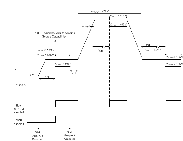 Figure 1. Timing Illustration for tVP, tST and tSTL, After Sink Attachment Negotiation to 12 V Then Back to 5 V. V(SOVP) and V(SUVP) are Disabled Around Voltage Transitions.
  Figure 2. Timing Illustration for tHR and tSR, After Sink Attachment with Persistent TJ > TJ1
 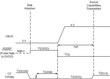 Figure 3. Timing Illustration for tCcDeb and tVP, Under Persistent Fault Condition
  Figure 4. Timing Illustration for tSH and tVP, with VBUS Shorted to Ground
 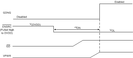 Figure 5. Timing Illustration for tON
 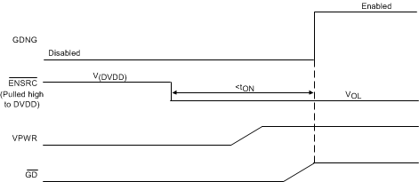 Figure 6. Timing Illustration for tON
 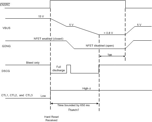 Figure 7. Timing Diagram for ENSRC and GDNG After Receiving a Hard Reset
 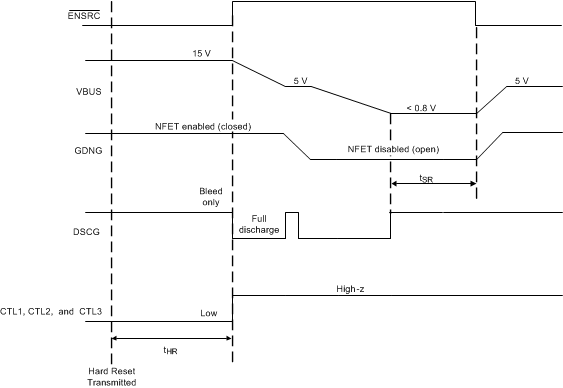 Figure 8. Timing Diagram for ENSRC and GDNG After Transmitting a Hard Reset