ZHCSGV1C June 2017 – March 2018 TPS25740B
PRODUCTION DATA.
- 1 特性
- 2 应用
- 3 说明
- 4 修订历史记录
- 5 Device Comparison Table
- 6 Pin Configuration and Functions
- 7 Specifications
-
8 Detailed Description
- 8.1 Overview
- 8.2 Functional Block Diagram
- 8.3
Feature Description
- 8.3.1 ENSRC
- 8.3.2 USB Type-C CC Logic (CC1, CC2)
- 8.3.3 USB PD BMC Transmission (CC1, CC2, VTX)
- 8.3.4 USB PD BMC Reception (CC1, CC2)
- 8.3.5 Discharging (DSCG, VPWR)
- 8.3.6 Configuring Voltage Capabilities (HIPWR)
- 8.3.7 Configuring Power Capabilities (PSEL, PCTRL, HIPWR)
- 8.3.8 Gate Driver (GDNG, GDNS)
- 8.3.9 Fault Monitoring and Protection
- 8.3.10 Voltage Control (CTL1, CTL2,CTL3)
- 8.3.11 Sink Attachment Indicator (DVDD)
- 8.3.12 Power Supplies (VAUX, VDD, VPWR, DVDD)
- 8.3.13 Grounds (AGND, GND)
- 8.3.14 Output Power Supply (DVDD)
- 8.4 Device Functional Modes
-
9 Application and Implementation
- 9.1
Application Information
- 9.1.1 System-Level ESD Protection
- 9.1.2 Using ENSRC to Enable the Power Supply upon Sink Attachment
- 9.1.3 Use of GD Internal Clamp
- 9.1.4 Resistor Divider on GD for Programmable Start Up
- 9.1.5 Selection of the CTL1, CTL2, and CTL3 Resistors (R(FBL1), R(FBL2), and R(FBL3))
- 9.1.6 Voltage Transition Requirements
- 9.1.7 VBUS Slew Control using GDNG C(SLEW)
- 9.1.8 Tuning OCP using RF and CF
- 9.2 Typical Applications
- 9.3 System Examples
- 9.1
Application Information
- 10Power Supply Recommendations
- 11Layout
- 12器件和文档支持
- 13机械、封装和可订购信息
8.3.9.1 Over/Under Voltage (VBUS)
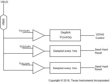
The TPS25740B uses the VBUS pin to monitor for overvoltage or undervoltage conditions and implement the fast-OVP, slow-OVP and slow-UVP features.
 Figure 34. Voltage Monitoring Circuits
 If an over-voltage condition is sensed by the Fast OVP mechanism, GDNG is disabled within tFOVP + tFOVPDG, then a Hard Reset is transmitted and the VBUS discharge sequence is started. At power up the voltage trip point is set to V(FOVP) (5 V contract). When a contract is negotiated the trip point is set to the corresponding V(FOVP) value.
The devices employ another slow over-voltage protection mechanism as well that sends the Hard Reset before disabling the external NFET. It catches many OV events before the Fast OVP mechanism. During intentional positive voltage transitions, this mechanism is disabled (see Figure 1). However, tVP after the external NFET has been enabled, if the voltage on the VBUS pin exceeds V(SOVP) then a Hard Reset is transmitted to the Sink and the VBUS discharge sequence is started.
The devices employ a slow under-voltage protection mechanism as well that sends the Hard Reset before disabling GDNG. During intentional negative voltage transitions, this mechanism is disabled (see Figure 1). However, tVP after the external NFET has been enabled if the voltage on the VBUS pin falls below V(SUVP), then a Hard Reset is transmitted to the Sink and the VBUS discharge sequence is started.