SLAS354C September 2001 – September 2015 TLV2553
PRODUCTION DATA.
- 1 Features
- 2 Applications
- 3 Description
- 4 Revision History
- 5 Pin Configuration and Functions
-
6 Specifications
- 6.1 Absolute Maximum Ratings
- 6.2 ESD Ratings
- 6.3 Recommended Operating Conditions
- 6.4 Thermal Information
- 6.5 Electrical Characteristics
- 6.6 External Reference Specifications
- 6.7 Operating Characteristics
- 6.8 Timing Requirements: VREF+ = 5 V
- 6.9 Timing Requirements: VREF+ = 2.5 V
- 6.10 Typical Characteristics
- 7 Parameter Measurement Information
-
8 Detailed Description
- 8.1 Overview
- 8.2 Functional Block Diagram
- 8.3 Feature Description
- 8.4
Device Functional Modes
- 8.4.1 Converter Operation
- 8.4.2 Data I/O Cycle
- 8.4.3 Sampling Cycle
- 8.4.4 Conversion Cycle
- 8.4.5 Power Up and Initialization
- 8.4.6 Data Input
- 8.4.7 Data Input—Address/Command Bits
- 8.4.8 Data Output Length
- 8.4.9 LSB Out First
- 8.4.10 Bipolar Output Format
- 8.4.11 EOC Output
- 8.4.12 Chip-Select Input (CS)
- 8.4.13 Power-Down Features
- 9 Application and Implementation
- 10Power Supply Recommendations
- 11Layout
- 12Device and Documentation Support
- 13Mechanical, Packaging, and Orderable Information
封装选项
机械数据 (封装 | 引脚)
散热焊盘机械数据 (封装 | 引脚)
- PW|20
订购信息
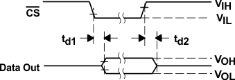
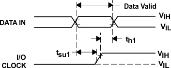
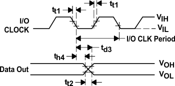
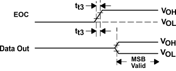
7 Parameter Measurement Information
 Figure 31. DATA OUT to Hi-Z Voltage Waveforms
 Figure 32. DATA IN and I/O CLOCK Voltage
 Figure 33. CS and I/O CLOCK
 Voltage Waveforms
 Figure 34. I/O CLOCK and DATA OUT
 Voltage Waveforms
 Figure 35. I/O CLOCK and EOC
 Voltage Waveforms
 Figure 36. EOC and DATA OUT
 Voltage Waveforms
 Figure 37. CS and EOC Waveforms
 Figure 38. I/O CLOCK and DATA OUT Voltage