ZHCSFY4 December 2016 TAS5780M
PRODUCTION DATA.
- 1 特性
- 2 应用
- 3 说明
- 4 修订历史记录
- 5 Device Comparison Table
- 6 Pin Configuration and Functions
-
7 Specifications
- 7.1 Absolute Maximum Ratings
- 7.2 ESD Ratings
- 7.3 Recommended Operating Conditions
- 7.4 Thermal Information
- 7.5 Electrical Characteristics
- 7.6 Power Dissipation Characteristics
- 7.7 MCLK Timing
- 7.8 Serial Audio Port Timing - Slave Mode
- 7.9 Serial Audio Port Timing - Master Mode
- 7.10 I2C Bus Timing - Standard
- 7.11 I2C Bus Timing - Fast
- 7.12 SPK_MUTE Timing
- 7.13 Typical Characteristics
- 8 Parametric Measurement Information
-
9 Detailed Description
- 9.1 Overview
- 9.2 Functional Block Diagram
- 9.3
Feature Description
- 9.3.1 Power-on-Reset (POR) Function
- 9.3.2 Device Clocking
- 9.3.3
Serial Audio Port
- 9.3.3.1 Clock Master Mode from Audio Rate Master Clock
- 9.3.3.2 Clock Master from a Non-Audio Rate Master Clock
- 9.3.3.3 Clock Slave Mode with 4-Wire Operation (SCLK, MCLK, LRCK/FS, SDIN)
- 9.3.3.4 Clock Slave Mode with SCLK PLL to Generate Internal Clocks (3-Wire PCM)
- 9.3.3.5 Serial Audio Port - Data Formats and Bit Depths
- 9.3.3.6 Input Signal Sensing (Power-Save Mode)
- 9.3.4 Enable Device
- 9.3.5 Volume Control
- 9.3.6 Adjustable Amplifier Gain and Switching Frequency Selection
- 9.3.7
Error Handling and Protection Suite
- 9.3.7.1 Device Overtemperature Protection
- 9.3.7.2 SPK_OUTxx Overcurrent Protection
- 9.3.7.3 Internal VAVDD Undervoltage-Error Protection
- 9.3.7.4 Internal VPVDD Undervoltage-Error Protection
- 9.3.7.5 Internal VPVDD Overvoltage-Error Protection
- 9.3.7.6 External Undervoltage-Error Protection
- 9.3.7.7 Internal Clock Error Notification (CLKE)
- 9.3.8 GPIO Port and Hardware Control Pins
- 9.3.9 I2C Communication Port
- 9.4 Device Functional Modes
- 9.5
Programming
- 9.5.1 Audio Processing Features
- 9.5.2 Processing Block Description
- 9.5.3 Other Processing Block Features
- 9.5.4 Checksum
- 10Application and Implementation
- 11Power Supply Recommendations
- 12Layout
-
13Register Maps
- 13.1
Registers - Page 0
- 13.1.1 Register 1 (0x01)
- 13.1.2 Register 2 (0x02)
- 13.1.3 Register 3 (0x03)
- 13.1.4 Register 4 (0x04)
- 13.1.5 Register 5 (0x05)
- 13.1.6 Register 6 (0x06)
- 13.1.7 Register 7 (0x07)
- 13.1.8 Register 8 (0x08)
- 13.1.9 Register 9 (0x09)
- 13.1.10 Register 10 (0x0A)
- 13.1.11 Register 12 (0x0C)
- 13.1.12 Register 13 (0x0D)
- 13.1.13 Register 14 (0x0E)
- 13.1.14 Register 15 (0x0F)
- 13.1.15 Register 16 (0x10)
- 13.1.16 Register 17 (0x11)
- 13.1.17 Register 18 (0x12)
- 13.1.18 Register 19 (0x13)
- 13.1.19 Register 20 (0x14)
- 13.1.20 Register 21 (0x15)
- 13.1.21 Register 22 (0x16)
- 13.1.22 Register 23 (0x17)
- 13.1.23 Register 24 (0x18)
- 13.1.24 Register 25 (0x19)
- 13.1.25 Register 26 (0x1A)
- 13.1.26 Register 27 (0x1B)
- 13.1.27 Register 28 (0x1C)
- 13.1.28 Register 29 (0x1D)
- 13.1.29 Register 30 (0x1E)
- 13.1.30 Register 31 (0x1F)
- 13.1.31 Register 32 (0x20)
- 13.1.32 Register 33 (0x21)
- 13.1.33 Register 34 (0x22)
- 13.1.34 Register 35 (0x23)
- 13.1.35 Register 37 (0x25)
- 13.1.36 Register 38 (0x26)
- 13.1.37 Register 39 (0x27)
- 13.1.38 Register 40 (0x28)
- 13.1.39 Register 41 (0x29)
- 13.1.40 Register 42 (0x2A)
- 13.1.41 Register 43 (0x2B)
- 13.1.42 Register 44 (0x2C)
- 13.1.43 Register 45 (0x2D)
- 13.1.44 Register 46 (0x2E)
- 13.1.45 Register 47 (0x2F)
- 13.1.46 Register 48 (0x30)
- 13.1.47 Register 49 (0x31)
- 13.1.48 Register 50 (0x32)
- 13.1.49 Register 51 (0x33)
- 13.1.50 Register 52 (0x34)
- 13.1.51 Register 53 (0x35)
- 13.1.52 Register 59 (0x3B)
- 13.1.53 Register 60 (0x3C)
- 13.1.54 Register 61 (0x3D)
- 13.1.55 Register 62 (0x3E)
- 13.1.56 Register 63 (0x3F)
- 13.1.57 Register 64 (0x40)
- 13.1.58 Register 65 (0x41)
- 13.1.59 Register 66 (0x42)
- 13.1.60 Register 67 (0x43)
- 13.1.61 Register 68 (0x44)
- 13.1.62 Register 69 (0x45)
- 13.1.63 Register 70 (0x46)
- 13.1.64 Register 71 (0x47)
- 13.1.65 Register 72 (0x48)
- 13.1.66 Register 73 (0x49)
- 13.1.67 Register 74 (0x4A)
- 13.1.68 Register 75 (0x4B)
- 13.1.69 Register 76 (0x4C)
- 13.1.70 Register 78 (0x4E)
- 13.1.71 Register 79 (0x4F)
- 13.1.72 Register 80 (0x50)
- 13.1.73 Register 81 (0x51)
- 13.1.74 Register 82 (0x52)
- 13.1.75 Register 83 (0x53)
- 13.1.76 Register 84 (0x54)
- 13.1.77 Register 85 (0x55)
- 13.1.78 Register 86 (0x56)
- 13.1.79 Register 87 (0x57)
- 13.1.80 Register 88 (0x58)
- 13.1.81 Register 89 (0x59)
- 13.1.82 Register 91 (0x5B)
- 13.1.83 Register 92 (0x5C)
- 13.1.84 Register 93 (0x5D)
- 13.1.85 Register 94 (0x5E)
- 13.1.86 Register 95 (0x5F)
- 13.1.87 Register 96 (0x60)
- 13.1.88 Register 97 (0x61)
- 13.1.89 Register 98 (0x62)
- 13.1.90 Register 99 (0x63)
- 13.1.91 Register 100 (0x64)
- 13.1.92 Register 101 (0x65)
- 13.1.93 Register 102 (0x66)
- 13.1.94 Register 103 (0x67)
- 13.1.95 Register 104 (0x68)
- 13.1.96 Register 105 (0x69)
- 13.1.97 Register 106 (0x6A)
- 13.1.98 Register 107 (0x6B)
- 13.1.99 Register 108 (0x6C)
- 13.1.100 Register 109 (0x6D)
- 13.1.101 Register 110 (0x6E)
- 13.1.102 Register 111 (0x6F)
- 13.1.103 Register 112 (0x70)
- 13.1.104 Register 113 (0x71)
- 13.1.105 Register 114 (0x72)
- 13.1.106 Register 115 (0x73)
- 13.1.107 Register 118 (0x76)
- 13.1.108 Register 119 (0x77)
- 13.1.109 Register 120 (0x78)
- 13.1.110 Register 121 (0x79)
- 13.2
Registers - Page 1
- 13.2.1 Register 1 (0x01)
- 13.2.2 Register 2 (0x02)
- 13.2.3 Register 3 (0x03)
- 13.2.4 Register 4 (0x04)
- 13.2.5 Register 5 (0x05)
- 13.2.6 Register 6 (0x06)
- 13.2.7 Register 7 (0x07)
- 13.2.8 Register 8 (0x08)
- 13.2.9 Register 9 (0x09)
- 13.2.10 Register 10 (0x0A)
- 13.2.11 Register 11 (0x0B)
- 13.2.12 Register 12 (0x0C)
- 13.2.13 Register 13 (0x0D)
- 13.2.14 Register 14 (0x0E)
- 13.2.15 Register 15 (0x0F)
- 13.3
Registers - Page 253
- 13.3.1 Register 1 (0x01)
- 13.3.2 Register 2 (0x02)
- 13.3.3 Register 3 (0x03)
- 13.3.4 Register 4 (0x04)
- 13.3.5 Register 5 (0x05)
- 13.3.6 Register 6 (0x06)
- 13.3.7 Register 7 (0x07)
- 13.3.8 Register 8 (0x08)
- 13.3.9 Register 9 (0x09)
- 13.3.10 Register 10 (0x0A)
- 13.3.11 Register 11 (0x0B)
- 13.3.12 Register 12 (0x0C)
- 13.3.13 Register 13 (0x0D)
- 13.3.14 Register 14 (0x0E)
- 13.3.15 Register 15 (0x0F)
- 13.3.16 Register 16 (0x10)
- 13.3.17 Register 17 (0x11)
- 13.3.18 Register 18 (0x12)
- 13.3.19 Register 19 (0x13)
- 13.3.20 Register 20 (0x14)
- 13.3.21 Register 21 (0x15)
- 13.3.22 Register 2 (0x16)
- 13.3.23 Register 23 (0x17)
- 13.3.24 Register 24 (0x18)
- 13.3.25 Register 25 (0x19)
- 13.3.26 Register 26 (0x1A)
- 13.3.27 Register 27 (0x1B)
- 13.3.28 Register 28 (0x1C)
- 13.3.29 Register 29 (0x1D)
- 13.3.30 Register 30 (0x1E)
- 13.3.31 Register 31 (0x1F)
- 13.3.32 Register 32 (0x20)
- 13.3.33 Register 33 (0x21)
- 13.3.34 Register 34 (0x22)
- 13.3.35 Register 35 (0x23)
- 13.3.36 Register 36 (0x24)
- 13.3.37 Register 37 (0x25)
- 13.3.38 Register 38 (0x26)
- 13.3.39 Register 39 (0x27)
- 13.3.40 Register 40 (0x28)
- 13.3.41 Register 41 (0x29)
- 13.3.42 Register 42 (0x2A)
- 13.3.43 Register 43 (0x2B)
- 13.3.44 Register 44 (0x2C)
- 13.3.45 Register 63 (0x3F)
- 13.3.46 Register 64 (0x40)
- 13.3.47 Register 65 (0x41)
- 13.3.48 Register 70 (0x46)
- 13.3.49 Register 71 (0x47)
- 13.3.50 Register 72 (0x48)
- 13.3.51 Register 73 (0x49)
- 13.3.52 Register 74 (0x4A)
- 13.3.53 Register 75 (0x4B)
- 13.3.54 Register 76 (0x4C)
- 13.3.55 Register 77 (0x4D)
- 13.3.56 Register 78 (0x4E)
- 13.3.57 Register 79 (0x4F)
- 13.3.58 Register 80 (0x50)
- 13.3.59 Register 81 (0x51)
- 13.3.60 Register 82 (0x52)
- 13.3.61 Register 83 (0x53)
- 13.3.62 Register 84 (0x54)
- 13.3.63 Register 85 (0x55)
- 13.3.64 Register 86 (0x56)
- 13.3.65 Register 87 (0x57)
- 13.3.66 Register 88 (0x58)
- 13.3.67 Register 89 (0x59)
- 13.3.68 Register 90 (0x5A)
- 13.3.69 Register 91 (0x5B)
- 13.3.70 Register 92 (0x5C)
- 13.3.71 Register 93 (0x5D)
- 13.4 DSP Memory Map
- 13.1
Registers - Page 0
- 14器件和文档支持
- 15机械、封装和可订购信息
9 Detailed Description
9.1 Overview
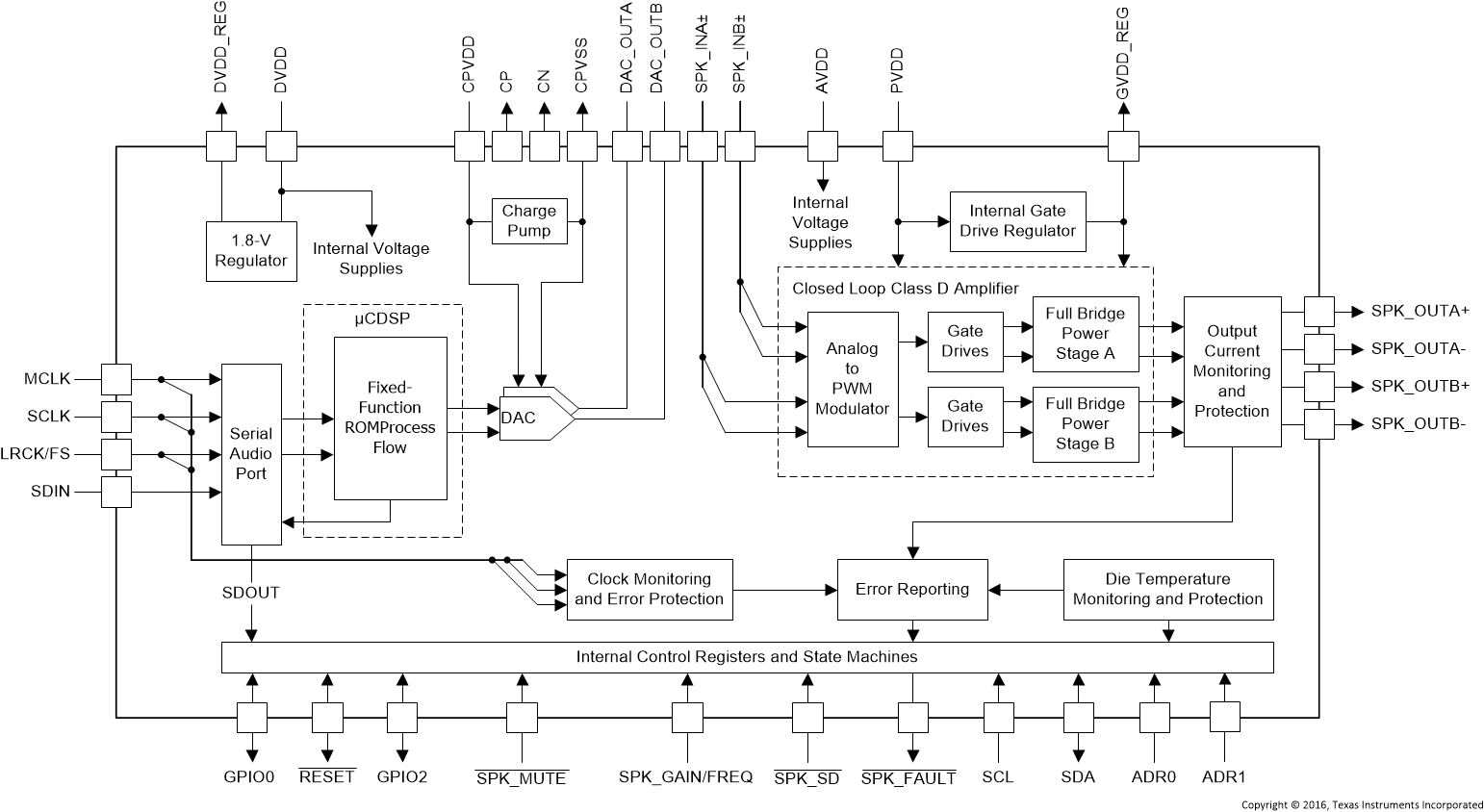
The TAS5780M device integrates 4 main building blocks together into a single cohesive device that maximizes sound quality, flexibility, and ease of use. The 4 main building blocks are listed below:
- A stereo audio DAC, boasting a strong Burr-Brown heritage with a highly flexible serial audio port.
- A µCDSP audio processing core, with a pre-programmed ROM image.
- A flexible closed-loop amplifier capable of operating in stereo or mono, at several different switching frequencies, and with a variety of output voltages and loads.
- An I2C control port for communication with the device
The device requires only two power supplies for proper operation. A DVDD supply is required to power the low-voltage digital and analog circuitry. Another supply, called PVDD, is required to provide power to the output stage of the audio amplifier. The operating range for these supplies is shown in the Recommended Operating Conditions table.
Communication with the device is accomplished through the I2C control port. A speaker amplifier fault line is also provided to notify a system controller of the occurrence of an overtemperature, overcurrent, overvoltage, or undervoltage. Two digital GPIO pins are available for use. In the fixed function ROM image of the TAS5780M, the GPIO2 pin is used as an SDOUT terminal. The other GPIO is unused.
The µCDSP audio processing core is pre-programmed with a configurable DSP program. The RD GUI provides a means by which to manipulate the controls associated with that Process Flow.
9.2 Functional Block Diagram
9.3 Feature Description
9.3.1 Power-on-Reset (POR) Function
The TAS5780M device has a power-on reset function. The power-on reset feature resets all of the registers to their default configuration as the device is powering up. When the low-voltage power supply used to power DVDD, AVDD, and CPVDD exceeds the POR threshold, the device sets all of the internal registers to their default values and holds them there until the device receives valid MCLK, SCLK, and LRCK/FS toggling for a period of approximately 4 ms. After the toggling period has passed, the internal reset of the registers is removed and the registers can be programmed via the I2C Control Port.
9.3.2 Device Clocking
The TAS5780M devices have flexible systems for clocking. Internally, the device requires a number of clocks, mostly at related clock rates to function correctly. All of these clocks can be derived from the Serial Audio Interface in one form or another.
 Figure 56. Audio Flow with Respective Clocks
Figure 56 shows the basic data flow at basic sample rate (fS). When the data is brought into the serial audio interface, the data is processed, interpolated and modulated to 128 × fS before arriving at the current segments for the final digital to analog conversion.
Figure 57 shows the clock tree.
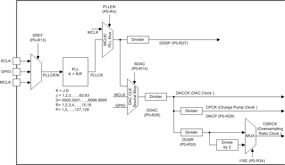 Figure 57. TAS5780M Clock Distribution Tree
The Serial Audio Interface typically has 4 connection pins which are listed as follows:
- MCLK (System Master Clock)
- SCLK (Bit Clock)
- LRCK/FS (Left Right Word Clock and Frame Sync)
- SDIN (Input Data)
- The output data, SDOUT, is presented on one of the GPIO pins.
- See the GPIO Port and Hardware Control Pins section)
The device has an internal PLL that is used to take either MCLK or SCLK and create the higher rate clocks required by the DSP and the DAC clock.
In situations where the highest audio performance is required, bringing MCLK to the device along with SCLK and LRCK/FS is recommended. The device should be configured so that the PLL is only providing a clock source to the DSP. All other clocks are then a division of the incoming MCLK. To enable the MCLK as the main source clock, with all others being created as divisions of the incoming MCLK, set the DAC CLK source Mux (SDAC in Figure 57) to use MCLK as a source, rather than the output of the MCLK/PLL Mux.
9.3.3 Serial Audio Port
9.3.3.1 Clock Master Mode from Audio Rate Master Clock
In Master Mode, the device generates bit clock and left-right and frame sync clock and outputs them on the appropriate pins. To configure the device in master mode, first put the device into reset, then use registers SCLKO and LRKO (P0-R9). Then reset the LRCK/FS and SCLK divider counters using bits RSCLK and RLRK (P0-R12). Finally, exit reset.
Figure 58 shows a simplified serial port clock tree for the device in master mode.
 Figure 58. Simplified Clock Tree for MCLK Sourced Master Mode
In master mode, MCLK is an input and SCLK and LRCK/FS are outputs. SCLK and LRCK/FS are integer divisions of MCLK. Master mode with a non-audio rate master clock source requires external GPIO’s to use the PLL in standalone mode. The PLL should be configured to ensure that the on-chip processor can be driven at the maximum clock rate. The master mode of operation is described in the Clock Master from a Non-Audio Rate Master Clock section.
When used with audio rate master clocks, the register changes that should be done include switching the device into master mode, and setting the divider ratio. An example of the master mode of operations is using 24.576 MHz MCLK as a master clock source and driving the SCLK and LRCK/FS with integer dividers to create 48 kHz sample rate clock output. In master mode, the DAC section of the device is also running from the PLL output. The TAS5780M device is able to meet the specified audio performance while using the internal PLL. However, using the MCLK CMOS oscillator source will have less jitter than the PLL.
To switch the DAC clocks (SDAC in the Figure 57) the following registers should be modified
- Clock Tree Flex Mode (P253-R63 and P253-R64)
- DAC and OSR Source Clock Register (P0-R14). Set to 0x30 (MCLK input, and OSR is set to whatever the DAC source is)
- The DAC clock divider should be 16 fS.
- 16 × 48 kHz = 768 kHz
- 24.576 MHz (MCLK in) / 768 kHz = 32
- Therefore, the divide ratio for register DDAC (P0-R28) should be set to 32. The register mapping gives 0x00 = 1, therefore 32 must be converter to 0x1F (31dec).
9.3.3.2 Clock Master from a Non-Audio Rate Master Clock
The classic example here is running a 96-kHz sampling system. Given the clock tree for the device (shown in Figure 57), a non-audio clock rate cannot be brought into the MCLK to the PLL in master mode. Therefore, the PLL source must be configured to be a GPIO pin, and the output brought back into another GPIO pin.
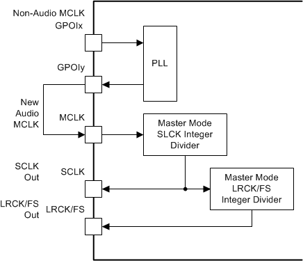 Figure 59. Generating Audio Clocks Using Non-Audio Clock Sources
The clock flow through the system is shown in Figure 59. The newly generated MCLK must be brought out of the device on a GPIO pin, then brought into the MCLK pin for integer division to create SCLK and LRCK/FS outputs.
NOTE
Pull-up resistors should be used on SCLK and LRCK/FS in master mode to ensure the device remains out of sleep mode.
9.3.3.3 Clock Slave Mode with 4-Wire Operation (SCLK, MCLK, LRCK/FS, SDIN)
The TAS5780M device requires a system clock to operate the digital interpolation filters and advanced segment DAC modulators. The system clock is applied at the MCLK input and supports up to 50 MHz. The TAS5780M device system-clock detection circuit automatically senses the system-clock frequency. Common audio sampling frequencies in the bands of 32 kHz, (44.1 – 48 kHz), (88.2 – 96 kHz) are supported.
NOTE
Values in the parentheses are grouped when detected, for example, 88.2 kHz and 96 kHz are detected as double rate, 32 kHz, 44.1 kHz and 48 kHz are detected as single rate and so on.
In the presence of a valid bit MCLK, SCLK and LRCK/FS, the device automatically configures the clock tree and PLL to drive the µCDSP as required.
The sampling frequency detector sets the clock for the digital filter, Delta Sigma Modulator (DSM) and the Negative Charge Pump (NCP) automatically. Table 2 shows examples of system clock frequencies for common audio sampling rates.
MCLK rates that are not common to standard audio clocks, between 1 MHz and 50 MHz, are supported by configuring various PLL and clock-divider registers directly. In slave mode, auto clock mode should be disabled using P0-R37. Additionally, the user can be required to ignore clock error detection if external clocks are not available for some time during configuration or if the clocks presented on the pins of the device are invalid. The extended programmability allows the device to operate in an advanced mode in which the device becomes a clock master and drive the host serial port with LRCK/FS and SCLK, from a non-audio related clock (for example, using a setting of 12 MHz to generate 44.1 kHz [LRCK/FS] and 2.8224 MHz [SCLK]).
Table 2 shows the timing requirements for the system clock input. For optimal performance, use a clock source with low phase jitter and noise. For MCLK timing requirements, refer to the Serial Audio Port Timing – Master Mode section.
Table 2. System Master Clock Inputs for Audio Related Clocks
| SAMPLING FREQUENCY |
SYSTEM CLOCK FREQUENCY (fMCLK) (MHz) | |||||
|---|---|---|---|---|---|---|
| 64 fS | 128 fS | 192 fS | 256 fS | 384 fS | 512 fS | |
| 8 kHz | See(1) | 1.024(2) | 1.536(2) | 2.048 | 3.072 | 4.096 |
| 16 kHz | 2.048(2) | 3.072(2) | 4.096 | 6.144 | 8.192 | |
| 32 kHz | 4.096(2) | 6.144(2) | 8.192 | 12.288 | 16.384 | |
| 44.1 kHz | 5.6488(2) | 8.4672(2) | 11.2896 | 16.9344 | 22.5792 | |
| 48 kHz | 6.144(2) | 9.216(2) | 12.288 | 18.432 | 24.576 | |
| 88.2 kHz | 11.2896(2) | 16.9344 | 22.5792 | 33.8688 | 45.1584 | |
| 96 kHz | 12.288(2) | 18.432 | 24.576 | 36.864 | 49.152 | |
9.3.3.4 Clock Slave Mode with SCLK PLL to Generate Internal Clocks (3-Wire PCM)
9.3.3.4.1 Clock Generation using the PLL
The TAS5780M device supports a wide range of options to generate the required clocks as shown in Figure 57.
The clocks for the PLL require a source reference clock. This clock is sourced as the incoming SCLK or MCLK, a GPIO can also be used.
The source reference clock for the PLL reference clock is selected by programming the SRCREF value on P0-R13, D[6:4]. The TAS5780M device provides several programmable clock dividers to achieve a variety of sampling rates. See Figure 57.
If PLL functionality is not required, set the PLLEN value on P0-R4, D[0] to 0. In this situation, an external master clock is required.
Table 3. PLL Configuration Registers
| CLOCK MULTIPLEXER | ||
|---|---|---|
| REGISTER | FUNCTION | BITS |
| SREF | PLL Reference | B0-P0-R13-D[6:4] |
| DDSP | Clock divider | B0-P0-R27-D[6:0] |
| DSCLK | External SCLK Div | B0-P0-R32-D[6:0] |
| DLRK | External LRCK/FS Div | B0-P0-R33-D[7:0] |
9.3.3.4.2 PLL Calculation
The TAS5780M device has an on-chip PLL with fractional multiplication to generate the clock frequency required by the Digital Signal Processing blocks. The programmability of the PLL allows operation from a wide variety of clocks that may be available in the system. The PLL input (PLLCKIN) supports clock frequencies from 1 MHz to 50 MHz and is register programmable to enable generation of required sampling rates with fine precision.
The PLL is enabled by default. The PLL can be enabled by writing to P0-R4, D[0]. When the PLL is enabled, the PLL output clock PLLCK is given by Equation 1:

where
- R = 1, 2, 3,4, ... , 15, 16
- J = 4,5,6, . . . 63, and D = 0000, 0001, 0002, . . . 9999
- K = [J value].[D value]
- P = 1, 2, 3, ... 15
R, J, D, and P are programmable. J is the integer portion of K (the numbers to the left of the decimal point), while D is the fractional portion of K (the numbers to the right of the decimal point, assuming four digits of precision).
9.3.3.4.2.1 Examples:
- If K = 8.5, then J = 8, D = 5000
- If K = 7.12, then J = 7, D = 1200
- If K = 14.03, then J = 14, D = 0300
- If K = 6.0004, then J = 6, D = 0004
When the PLL is enabled and D = 0000, the following conditions must be satisfied:
- 1 MHz ≤ ( PLLCKIN / P ) ≤ 20 MHz
- 64 MHz ≤ (PLLCKIN x K x R / P ) ≤ 100 MHz
- 1 ≤ J ≤ 63
When the PLL is enabled and D ≠ 0000, the following conditions must be satisfied:
- 6.667 MHz ≤ PLLCLKIN / P ≤ 20 MHz
- 64 MHz ≤ (PLLCKIN x K x R / P ) ≤ 100 MHz
- 4 ≤ J ≤ 11
- R = 1
When the PLL is enabled,
- fS = (PLLCLKIN × K × R) / (2048 × P)
- The value of N is selected so that fS × N = PLLCLKIN x K x R / P is in the allowable range.
Example: MCLK = 12 MHz and fS = 44.1 kHz, (N=2048)
Select P = 1, R = 1, K = 7.5264, which results in J = 7, D = 5264
Example: MCLK = 12 MHz and fS = 48.0 kHz, (N=2048)
Select P = 1, R = 1, K = 8.192, which results in J = 8, D = 1920
Values are written to the registers in Table 4.
Table 4. PLL Registers
| DIVIDER | FUNCTION | BITS |
|---|---|---|
| PLLE | PLL enable | P0-R4, D[0] |
| PPDV | PLL P | P0-R20, D[3:0] |
| PJDV | PLL J | P0-R21, D[5:0] |
| PDDV | PLL D | P0-R22, D[5:0] |
| P0-R23, D[7:0] | ||
| PRDV | PLL R | P0-R24, D[3:0] |
Table 5. PLL Configuration Recommendations
| EQUATIONS | DESCRIPTION |
|---|---|
| fS (kHz) | Sampling frequency |
| RMCLK | Ratio between sampling frequency and MCLK frequency (MCLK frequency = RMCLK x sampling frequency) |
| MCLK (MHz) | System master clock frequency at MCLK input (pin 20) |
| PLL VCO (MHz) | PLL VCO frequency as PLLCK in Figure 57 |
| P | One of the PLL coefficients in Equation 1 |
| PLL REF (MHz) | Internal reference clock frequency which is produced by MCLK / P |
| M = K × R | The final PLL multiplication factor computed from K and R as described in Equation 1 |
| K = J.D | One of the PLL coefficients in Equation 1 |
| R | One of the PLL coefficients in Equation 1 |
| PLL fS | Ratio between fS and PLL VCO frequency (PLL VCO / fS) |
| DSP fS | Ratio between operating clock rate and fS (PLL fS / NMAC) |
| NMAC | The clock divider value in Table 3 |
| DSP CLK (MHz) | The operating frequency as DSPCK in Figure 57 |
| MOD fS | Ratio between DAC operating clock frequency and fS (PLL fS / NDAC) |
| MOD f (kHz) | DAC operating frequency as DACCK in |
| NDAC | DAC clock divider value in Table 3 |
| DOSR | OSR clock divider value in Table 3 for generating OSRCK in Figure 57. DOSR must be chosen so that MOD fS / DOSR = 16 for correct operation. |
| NCP | NCP (negative charge pump) clock divider value in Table 3 |
| CP f | Negative charge pump clock frequency (fS × MOD fS / NCP) |
| % Error | Percentage of error between PLL VCO / PLL fS and fS (mismatch error).
|
The previous equations explain how to calculate all necessary coefficients and controls to configure the PLL. Table 6 provides for easy reference to the recommended clock divider settings for the PLL as a Master Clock.
Table 6. Recommended Clock Divider Settings for PLL as Master Clock
| fS
(kHz) |
RMCLK | MCLK (MHz) |
PLL VCO (MHz) |
P | PLL REF (MHz) |
M = K×R | K = J×D | R | PLL fS | DSP fS | NMAC | DSP CLK (MHz) |
MOD fS | MOD f (kHz) |
NDAC | DOSR | % ERROR | NCP | CP f (kHz) |
|---|---|---|---|---|---|---|---|---|---|---|---|---|---|---|---|---|---|---|---|
| 8 | 128 | 1.024 | 98.304 | 1 | 1.024 | 96 | 48 | 2 | 12288 | 1024 | 12 | 8.192 | 768 | 6144 | 16 | 48 | 0 | 4 | 1536 |
| 192 | 1.536 | 98.304 | 1 | 1.536 | 64 | 32 | 2 | 12288 | 1024 | 12 | 8.192 | 768 | 6144 | 16 | 48 | 0 | 4 | 1536 | |
| 256 | 2.048 | 98.304 | 1 | 2.048 | 48 | 48 | 1 | 12288 | 1024 | 12 | 8.192 | 768 | 6144 | 16 | 48 | 0 | 4 | 1536 | |
| 384 | 3.072 | 98.304 | 3 | 1.024 | 96 | 48 | 2 | 12288 | 1024 | 12 | 8.192 | 768 | 6144 | 16 | 48 | 0 | 4 | 1536 | |
| 512 | 4.096 | 98.304 | 3 | 1.365 | 72 | 36 | 2 | 12288 | 1024 | 12 | 8.192 | 768 | 6144 | 16 | 48 | 0 | 4 | 1536 | |
| 768 | 6.144 | 98.304 | 3 | 2.048 | 48 | 48 | 1 | 12288 | 1024 | 12 | 8.192 | 768 | 6144 | 16 | 48 | 0 | 4 | 1536 | |
| 1024 | 8.192 | 98.304 | 3 | 2.731 | 36 | 36 | 1 | 12288 | 1024 | 12 | 8.192 | 768 | 6144 | 16 | 48 | 0 | 4 | 1536 | |
| 1152 | 9.216 | 98.304 | 9 | 1.024 | 96 | 48 | 2 | 12288 | 1024 | 12 | 8.192 | 768 | 6144 | 16 | 48 | 0 | 4 | 1536 | |
| 1536 | 12.288 | 98.304 | 9 | 1.365 | 72 | 36 | 2 | 12288 | 1024 | 12 | 8.192 | 768 | 6144 | 16 | 48 | 0 | 4 | 1536 | |
| 2048 | 16.384 | 98.304 | 9 | 1.82 | 54 | 54 | 1 | 12288 | 1024 | 12 | 8.192 | 768 | 6144 | 16 | 48 | 0 | 4 | 1536 | |
| 3072 | 24.576 | 98.304 | 9 | 2.731 | 36 | 36 | 1 | 12288 | 1024 | 12 | 8.192 | 768 | 6144 | 16 | 48 | 0 | 4 | 1536 | |
| 11.025 | 128 | 1.4112 | 90.3168 | 1 | 1.411 | 64 | 32 | 2 | 8192 | 1024 | 8 | 11.2896 | 512 | 5644.8 | 16 | 32 | 0 | 4 | 1411.2 |
| 192 | 2.1168 | 90.3168 | 3 | 0.706 | 128 | 32 | 4 | 8192 | 1024 | 8 | 11.2896 | 512 | 5644.8 | 16 | 32 | 0 | 4 | 1411.2 | |
| 256 | 2.8224 | 90.3168 | 1 | 2.822 | 32 | 32 | 1 | 8192 | 1024 | 8 | 11.2896 | 512 | 5644.8 | 16 | 32 | 0 | 4 | 1411.2 | |
| 384 | 4.2336 | 90.3168 | 3 | 1.411 | 64 | 32 | 2 | 8192 | 1024 | 8 | 11.2896 | 512 | 5644.8 | 16 | 32 | 0 | 4 | 1411.2 | |
| 512 | 5.6448 | 90.3168 | 3 | 1.882 | 48 | 48 | 1 | 8192 | 1024 | 8 | 11.2896 | 512 | 5644.8 | 16 | 32 | 0 | 4 | 1411.2 | |
| 768 | 8.4672 | 90.3168 | 3 | 2.822 | 32 | 32 | 1 | 8192 | 1024 | 8 | 11.2896 | 512 | 5644.8 | 16 | 32 | 0 | 4 | 1411.2 | |
| 1024 | 11.2896 | 90.3168 | 3 | 3.763 | 24 | 24 | 1 | 8192 | 1024 | 8 | 11.2896 | 512 | 5644.8 | 16 | 32 | 0 | 4 | 1411.2 | |
| 1152 | 12.7008 | 90.3168 | 9 | 1.411 | 64 | 32 | 2 | 8192 | 1024 | 8 | 11.2896 | 512 | 5644.8 | 16 | 32 | 0 | 4 | 1411.2 | |
| 1536 | 16.9344 | 90.3168 | 9 | 1.882 | 48 | 48 | 1 | 8192 | 1024 | 8 | 11.2896 | 512 | 5644.8 | 16 | 32 | 0 | 4 | 1411.2 | |
| 2048 | 22.5792 | 90.3168 | 9 | 2.509 | 36 | 36 | 1 | 8192 | 1024 | 8 | 11.2896 | 512 | 5644.8 | 16 | 32 | 0 | 4 | 1411.2 | |
| 3072 | 33.8688 | 90.3168 | 9 | 3.763 | 24 | 24 | 1 | 8192 | 1024 | 8 | 11.2896 | 512 | 5644.8 | 16 | 32 | 0 | 4 | 1411.2 | |
| 16 | 64 | 1.024 | 98.304 | 1 | 1.024 | 96 | 48 | 2 | 6144 | 1024 | 6 | 16.384 | 384 | 6144 | 16 | 24 | 0 | 4 | 1536 |
| 128 | 2.048 | 98.304 | 1 | 2.048 | 48 | 48 | 1 | 6144 | 1024 | 6 | 16.384 | 384 | 6144 | 16 | 24 | 0 | 4 | 1536 | |
| 192 | 3.072 | 98.304 | 1 | 3.072 | 32 | 32 | 1 | 6144 | 1024 | 6 | 16.384 | 384 | 6144 | 16 | 24 | 0 | 4 | 1536 | |
| 256 | 4.096 | 98.304 | 1 | 4.096 | 24 | 24 | 1 | 6144 | 1024 | 6 | 16.384 | 384 | 6144 | 16 | 24 | 0 | 4 | 1536 | |
| 384 | 6.144 | 98.304 | 3 | 2.048 | 48 | 48 | 1 | 6144 | 1024 | 6 | 16.384 | 384 | 6144 | 16 | 24 | 0 | 4 | 1536 | |
| 512 | 8.192 | 98.304 | 3 | 2.731 | 36 | 36 | 1 | 6144 | 1024 | 6 | 16.384 | 384 | 6144 | 16 | 24 | 0 | 4 | 1536 | |
| 768 | 12.288 | 98.304 | 3 | 4.096 | 24 | 24 | 1 | 6144 | 1024 | 6 | 16.384 | 384 | 6144 | 16 | 24 | 0 | 4 | 1536 | |
| 1024 | 16.384 | 98.304 | 3 | 5.461 | 18 | 18 | 1 | 6144 | 1024 | 6 | 16.384 | 384 | 6144 | 16 | 24 | 0 | 4 | 1536 | |
| 1152 | 18.432 | 98.304 | 3 | 6.144 | 16 | 16 | 1 | 6144 | 1024 | 6 | 16.384 | 384 | 6144 | 16 | 24 | 0 | 4 | 1536 | |
| 1536 | 24.576 | 98.304 | 9 | 2.731 | 36 | 36 | 1 | 6144 | 1024 | 6 | 16.384 | 384 | 6144 | 16 | 24 | 0 | 4 | 1536 | |
| 2048 | 32.768 | 98.304 | 9 | 3.641 | 27 | 27 | 1 | 6144 | 1024 | 6 | 16.384 | 384 | 6144 | 16 | 24 | 0 | 4 | 1536 | |
| 3072 | 49.152 | 98.304 | 9 | 5.461 | 18 | 18 | 1 | 6144 | 1024 | 6 | 16.384 | 384 | 6144 | 16 | 24 | 0 | 4 | 1536 | |
| 22.05 | 64 | 1.4112 | 90.3168 | 1 | 1.411 | 64 | 32 | 2 | 4096 | 1024 | 4 | 22.5792 | 256 | 5644.8 | 16 | 16 | 0 | 4 | 1411.2 |
| 128 | 2.8224 | 90.3168 | 1 | 2.822 | 32 | 32 | 1 | 4096 | 1024 | 4 | 22.5792 | 256 | 5644.8 | 16 | 16 | 0 | 4 | 1411.2 | |
| 192 | 4.2336 | 90.3168 | 3 | 1.411 | 64 | 32 | 2 | 4096 | 1024 | 4 | 22.5792 | 256 | 5644.8 | 16 | 16 | 0 | 4 | 1411.2 | |
| 256 | 5.6448 | 90.3168 | 1 | 5.645 | 16 | 16 | 1 | 4096 | 1024 | 4 | 22.5792 | 256 | 5644.8 | 16 | 16 | 0 | 4 | 1411.2 | |
| 384 | 8.4672 | 90.3168 | 3 | 2.822 | 32 | 32 | 1 | 4096 | 1024 | 4 | 22.5792 | 256 | 5644.8 | 16 | 16 | 0 | 4 | 1411.2 | |
| 512 | 11.2896 | 90.3168 | 3 | 3.763 | 24 | 24 | 1 | 4096 | 1024 | 4 | 22.5792 | 256 | 5644.8 | 16 | 16 | 0 | 4 | 1411.2 | |
| 768 | 16.9344 | 90.3168 | 3 | 5.645 | 16 | 16 | 1 | 4096 | 1024 | 4 | 22.5792 | 256 | 5644.8 | 16 | 16 | 0 | 4 | 1411.2 | |
| 1024 | 22.5792 | 90.3168 | 3 | 7.526 | 12 | 12 | 1 | 4096 | 1024 | 4 | 22.5792 | 256 | 5644.8 | 16 | 16 | 0 | 4 | 1411.2 | |
| 1152 | 25.4016 | 90.3168 | 9 | 2.822 | 32 | 32 | 1 | 4096 | 1024 | 4 | 22.5792 | 256 | 5644.8 | 16 | 16 | 0 | 4 | 1411.2 | |
| 1536 | 33.8688 | 90.3168 | 9 | 3.763 | 24 | 24 | 1 | 4096 | 1024 | 4 | 22.5792 | 256 | 5644.8 | 16 | 16 | 0 | 4 | 1411.2 | |
| 2048 | 45.1584 | 90.3168 | 9 | 5.018 | 18 | 18 | 1 | 4096 | 1024 | 4 | 22.5792 | 256 | 5644.8 | 16 | 16 | 0 | 4 | 1411.2 | |
| 32 | 32 | 1.024 | 98.304 | 1 | 1.024 | 96 | 48 | 2 | 3072 | 1024 | 3 | 32.768 | 192 | 6144 | 16 | 12 | 0 | 4 | 1536 |
| 48 | 1.536 | 98.304 | 1 | 1.536 | 64 | 16 | 4 | 3072 | 1024 | 3 | 32.768 | 192 | 6144 | 16 | 12 | 0 | 4 | 1536 | |
| 64 | 2.048 | 98.304 | 1 | 2.048 | 48 | 24 | 2 | 3072 | 1024 | 3 | 32.768 | 192 | 6144 | 16 | 12 | 0 | 4 | 1536 | |
| 128 | 4.096 | 98.304 | 1 | 4.096 | 24 | 24 | 1 | 3072 | 1024 | 3 | 32.768 | 192 | 6144 | 16 | 12 | 0 | 4 | 1536 | |
| 192 | 6.144 | 98.304 | 3 | 2.048 | 48 | 48 | 1 | 3072 | 1024 | 3 | 32.768 | 192 | 6144 | 16 | 12 | 0 | 4 | 1536 | |
| 256 | 8.192 | 98.304 | 2 | 4.096 | 24 | 24 | 1 | 3072 | 1024 | 3 | 32.768 | 192 | 6144 | 16 | 12 | 0 | 4 | 1536 | |
| 384 | 12.288 | 98.304 | 3 | 4.096 | 24 | 24 | 1 | 3072 | 1024 | 3 | 32.768 | 192 | 6144 | 16 | 12 | 0 | 4 | 1536 | |
| 512 | 16.384 | 98.304 | 3 | 5.461 | 18 | 18 | 1 | 3072 | 1024 | 3 | 32.768 | 192 | 6144 | 16 | 12 | 0 | 4 | 1536 | |
| 768 | 24.576 | 98.304 | 3 | 8.192 | 12 | 12 | 1 | 3072 | 1024 | 3 | 32.768 | 192 | 6144 | 16 | 12 | 0 | 4 | 1536 | |
| 1024 | 32.768 | 98.304 | 3 | 10.923 | 9 | 9 | 1 | 3072 | 1024 | 3 | 32.768 | 192 | 6144 | 16 | 12 | 0 | 4 | 1536 | |
| 1152 | 36.864 | 98.304 | 9 | 4.096 | 24 | 24 | 1 | 3072 | 1024 | 3 | 32.768 | 192 | 6144 | 16 | 12 | 0 | 4 | 1536 | |
| 1536 | 49.152 | 98.304 | 6 | 8.192 | 12 | 12 | 1 | 3072 | 1024 | 3 | 32.768 | 192 | 6144 | 16 | 12 | 0 | 4 | 1536 | |
| 44.1 | 32 | 1.4112 | 90.3168 | 1 | 1.411 | 64 | 32 | 2 | 2048 | 1024 | 2 | 45.1584 | 128 | 5644.8 | 16 | 8 | 0 | 4 | 1411.2 |
| 64 | 2.8224 | 90.3168 | 1 | 2.822 | 32 | 16 | 2 | 2048 | 1024 | 2 | 45.1584 | 128 | 5644.8 | 16 | 8 | 0 | 4 | 1411.2 | |
| 128 | 5.6448 | 90.3168 | 1 | 5.645 | 16 | 16 | 1 | 2048 | 1024 | 2 | 45.1584 | 128 | 5644.8 | 16 | 8 | 0 | 4 | 1411.2 | |
| 192 | 8.4672 | 90.3168 | 3 | 2.822 | 32 | 32 | 1 | 2048 | 1024 | 2 | 45.1584 | 128 | 5644.8 | 16 | 8 | 0 | 4 | 1411.2 | |
| 256 | 11.2896 | 90.3168 | 2 | 5.645 | 16 | 16 | 1 | 2048 | 1024 | 2 | 45.1584 | 128 | 5644.8 | 16 | 8 | 0 | 4 | 1411.2 | |
| 384 | 16.9344 | 90.3168 | 3 | 5.645 | 16 | 16 | 1 | 2048 | 1024 | 2 | 45.1584 | 128 | 5644.8 | 16 | 8 | 0 | 4 | 1411.2 | |
| 512 | 22.5792 | 90.3168 | 3 | 7.526 | 12 | 12 | 1 | 2048 | 1024 | 2 | 45.1584 | 128 | 5644.8 | 16 | 8 | 0 | 4 | 1411.2 | |
| 768 | 33.8688 | 90.3168 | 3 | 11.29 | 8 | 8 | 1 | 2048 | 1024 | 2 | 45.1584 | 128 | 5644.8 | 16 | 8 | 0 | 4 | 1411.2 | |
| 1024 | 45.1584 | 90.3168 | 3 | 15.053 | 6 | 6 | 1 | 2048 | 1024 | 2 | 45.1584 | 128 | 5644.8 | 16 | 8 | 0 | 4 | 1411.2 | |
| 48 | 32 | 1.536 | 98.304 | 1 | 1.536 | 64 | 32 | 2 | 2048 | 1024 | 2 | 49.152 | 128 | 6144 | 16 | 8 | 0 | 4 | 1536 |
| 64 | 3.072 | 98.304 | 1 | 3.072 | 32 | 16 | 2 | 2048 | 1024 | 2 | 49.152 | 128 | 6144 | 16 | 8 | 0 | 4 | 1536 | |
| 128 | 6.144 | 98.304 | 1 | 6.144 | 16 | 16 | 1 | 2048 | 1024 | 2 | 49.152 | 128 | 6144 | 16 | 8 | 0 | 4 | 1536 | |
| 192 | 9.216 | 98.304 | 3 | 3.072 | 32 | 32 | 1 | 2048 | 1024 | 2 | 49.152 | 128 | 6144 | 16 | 8 | 0 | 4 | 1536 | |
| 256 | 12.288 | 98.304 | 2 | 6.144 | 16 | 16 | 1 | 2048 | 1024 | 2 | 49.152 | 128 | 6144 | 16 | 8 | 0 | 4 | 1536 | |
| 384 | 18.432 | 98.304 | 3 | 6.144 | 16 | 16 | 1 | 2048 | 1024 | 2 | 49.152 | 128 | 6144 | 16 | 8 | 0 | 4 | 1536 | |
| 512 | 24.576 | 98.304 | 3 | 8.192 | 12 | 12 | 1 | 2048 | 1024 | 2 | 49.152 | 128 | 6144 | 16 | 8 | 0 | 4 | 1536 | |
| 768 | 36.864 | 98.304 | 3 | 12.288 | 8 | 8 | 1 | 2048 | 1024 | 2 | 49.152 | 128 | 6144 | 16 | 8 | 0 | 4 | 1536 | |
| 1024 | 49.152 | 98.304 | 3 | 16.384 | 6 | 6 | 1 | 2048 | 1024 | 2 | 49.152 | 128 | 6144 | 16 | 8 | 0 | 4 | 1536 | |
| 96 | 32 | 3.072 | 98.304 | 1 | 3.072 | 32 | 16 | 2 | 1024 | 512 | 2 | 49.152 | 64 | 6144 | 16 | 4 | 0 | 4 | 1536 |
| 48 | 4.608 | 98.304 | 3 | 1.536 | 64 | 32 | 2 | 1024 | 512 | 2 | 49.152 | 64 | 6144 | 16 | 4 | 0 | 4 | 1536 | |
| 64 | 6.144 | 98.304 | 1 | 6.144 | 16 | 8 | 2 | 1024 | 512 | 2 | 49.152 | 64 | 6144 | 16 | 4 | 0 | 4 | 1536 | |
| 128 | 12.288 | 98.304 | 2 | 6.144 | 16 | 16 | 1 | 1024 | 512 | 2 | 49.152 | 64 | 6144 | 16 | 4 | 0 | 4 | 1536 | |
| 192 | 18.432 | 98.304 | 3 | 6.144 | 16 | 16 | 1 | 1024 | 512 | 2 | 49.152 | 64 | 6144 | 16 | 4 | 0 | 4 | 1536 | |
| 256 | 24.576 | 98.304 | 4 | 6.144 | 16 | 16 | 1 | 1024 | 512 | 2 | 49.152 | 64 | 6144 | 16 | 4 | 0 | 4 | 1536 | |
| 384 | 36.864 | 98.304 | 6 | 6.144 | 16 | 16 | 1 | 1024 | 512 | 2 | 49.152 | 64 | 6144 | 16 | 4 | 0 | 4 | 1536 | |
| 512 | 49.152 | 98.304 | 8 | 6.144 | 16 | 16 | 1 | 1024 | 512 | 2 | 49.152 | 64 | 6144 | 16 | 4 | 0 | 4 | 1536 |
9.3.3.5 Serial Audio Port – Data Formats and Bit Depths
The serial audio interface port is a 3-wire serial port with the signals LRCK/FS (pin 25), SCLK (pin 23), and SDIN (pin 24). SCLK is the serial audio bit clock, used to clock the serial data present on SDIN into the serial shift register of the audio interface. Serial data is clocked into the TAS5780M device on the rising edge of SCLK. The LRCK/FS pin is the serial audio left/right word clock or frame sync when the device is operated in TDM Mode.
Table 7. TAS5780M Audio Data Formats, Bit Depths and Clock Rates
| FORMAT | DATA BITS | MAXIMUM LRCK/FS FREQUENCY (kHz) | MCLK RATE (fS) | SCLK RATE (fS) |
|---|---|---|---|---|
| I2S/LJ/RJ | 32, 24, 20, 16 | Up to 96 | 128 to 3072 (≤ 50 MHz) | 64, 48, 32 |
| TDM | 32, 24, 20, 16 | Up to 48 | 128 to 3072 | 125, 256 |
| 96 | 128 to 512 | 125, 256 |
The TAS5780M device requires the synchronization of LRCK/FS and system clock, but does not require a specific phase relation between LRCK/FS and system clock.
If the relationship between LRCK/FS and system clock changes more than ±5 MCLK, internal operation is initialized within one sample period and analog outputs are forced to the bipolar zero level until re-synchronization between LRCK/FS and system clock is completed.
If the relationship between LRCK/FS and SCLK are invalid more than 4 LRCK/FS periods, internal operation is initialized within one sample period and analog outputs are forced to the bipolar zero level until re-synchronization between LRCK/FS and SCLK is completed.
9.3.3.5.1 Data Formats and Master/Slave Modes of Operation
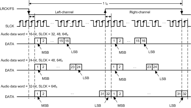
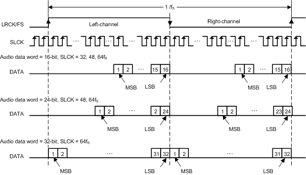
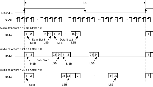
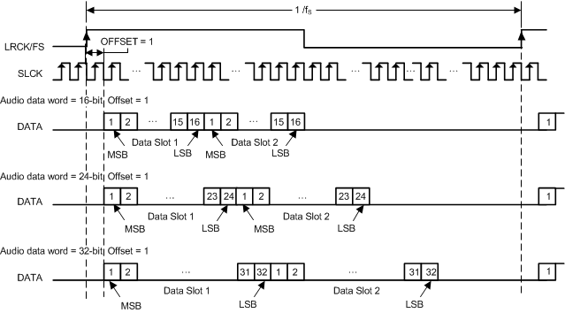
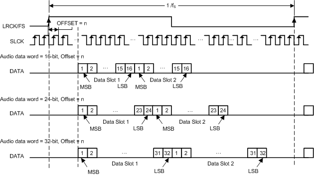
The TAS5780M device supports industry-standard audio data formats, including standard I2S and left-justified. Data formats are selected via Register (P0-R40). All formats require binary two's complement, MSB-first audio data; up to 32-bit audio data is accepted. The data formats are detailed in Figure 60 through Figure 65.
The TAS5780M device also supports right-justified, and TDM data. I2S, LJ, RJ, and TDM are selected using Register (P0-R40). All formats require binary 2s complement, MSB-first audio data. Up to 32 bits are accepted. Default setting is I2S and 24 bit word length. The I2S slave timing is shown in Figure 20.
shows a detailed timing diagram for the serial audio interface.
In addition to acting as a I2S slave, the TAS5780M device can act as an I2S master, by generating SCLK and LRCK/FS as outputs from the MCLK input. Table 8 lists the registers used to place the device into Master or Slave mode. Please refer to the Serial Audio Port Timing – Master Mode section for serial audio Interface timing requirements in Master Mode. For Slave Mode timing, please refer to the Serial Audio Port Timing – Slave Mode section.
Table 8. I2S Master Mode Registers
| REGISTER | FUNCTION |
|---|---|
| P0-R9-B0, B4, and B5 | I2S Master mode select |
| P0-R32-D[6:0] | SCLK divider and LRCK/FS divider |
| P0-R33-D[7:0] |
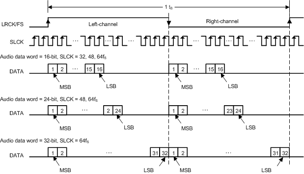 Figure 60. Left Justified Audio Data Format
The following data formats are only available in software mode.
9.3.3.6 Input Signal Sensing (Power-Save Mode)
The TAS5780M device has a zero-detect function. The zero-detect function can be applied to both channels of data as an AND function or an OR function, via controls provided in the control port in P0-R65-D[2:1].Continuous Zero data cycles are counted by LRCK/FS, and the threshold of decision for analog mute can be set by P0-R59, D[6:4] for the data which is clocked in on the left frame of an I2S signal or Slot 1 of a TDM signal and P0-R59, D[2:0] for the data which is clocked in on the right frame of an I2S signal or Slot 2 of a TDM signal as shown in Table 10. Default values are 0 for both channels.
In Hardware mode, the device uses default values.
Table 9. Zero Detection Mode
| ATMUTECTL | VALUE | FUNCTION |
|---|---|---|
| Bit : 2 | 0 | Zero data triggers for the two channels for zero detection are ORed together. |
| 1 (Default) | Zero data triggers for the two channels for zero detection are ANDed together. | |
| Bit : 1 | 0 | Zero detection and analog mute are disabled for the data clocked in on the right frame of an I2S signal or Slot 2 of a TDM signal. |
| 1 (Default) | Zero detection analog mute are enabled for the data clocked in on the right frame of an I2S signal or Slot 2 of a TDM signal. | |
| Bit : 0 | 0 | Zero detection analog mute are disabled for the data clocked in on the left frame of an I2S signal or Slot 1 of a TDM signal. |
| 1 (Default) | Zero detection analog mute are enabled for the data clocked in on the left frame of an I2S signal or Slot 1 of a TDM signal. |
Table 10. Zero Data Detection Time
| ATMUTETIML OR ATMA | NUMBER OF LRCK/FS CYCLES | TIME at 48 kHz |
|---|---|---|
| 0 0 0 | 1024 | 21 ms |
| 0 0 1 | 5120 | 106 ms |
| 0 1 0 | 10240 | 213 ms |
| 0 1 1 | 25600 | 533 ms |
| 1 0 0 | 51200 | 1.066 secs |
| 1 0 1 | 102400 | 2.133 secs |
| 1 1 0 | 256000 | 5.333 secs |
| 1 1 1 | 512000 | 10.66 secs |
9.3.4 Enable Device
To play audio after the device is powered up or reset the device must be enabled by writing book 0x00, page 0x00, register 0x02 to 0x00.
9.3.4.1 Example
The following is a sample script for enabling the device:
#Enable DUT
w 90 00 00 #Go to page 0
w 90 7f 00 #Go to book 0
w 90 02 00 #Enable device
9.3.5 Volume Control
9.3.5.1 DAC Digital Gain Control
A basic DAC digital gain control with range between 24 dB and –103 dB and mute is available on each channels by P0-R61-D[7:0] for SPK_OUTB± and P0-R62-D[7:0] for SPK_OUTA±. These volume controls all have 0.5 dB step programmability over most gain and attenuation ranges. Table 11 lists the detailed gain versus programmed setting for the basic volume control. Volume can be changed for both SPK_OUTB± and SPK_OUTA± at the same time or independently by P0-R61-D[1:0] . When D[1:0] set 00 (default), independent control is selected. When D[1:0] set 01, SPK_OUTA± accords with SPK_OUTB± volume. When D[1:0] set 10, SPK_OUTA± volume controls the volume for both channels. To set D[1:0] to 11 is prohibited.
Table 11. DAC Digital Gain Control Settings
| GAIN SETTING | BINARY DATA | GAIN (dB) | COMMENTS |
|---|---|---|---|
| 0 | 0000-0000 | 24.0 | Positive maximum |
| 1 | 0000-0001 | 23.5 | |
| . . . |
. . . |
. . . |
|
| 46 | 0010-1110 | 1.0 | |
| 47 | 0010-1111 | 0.5 | |
| 48 | 0011-0000 | 0.0 | No attenuation (default) |
| 49 | 0011-0001 | –0.5 | |
| 50 | 0011-0010 | –1.0 | |
| 51 | 0011-0011 | –1.5 | |
| . . . |
. . . |
. . . |
|
| 253 | 1111-1101 | –102.5 | |
| 254 | 1111-1110 | –103 | Negative maximum |
| 255 | 1111-1111 | –  |
Negative infinite (Mute) |
Ramp-up frequency and ramp-down frequency can be controlled by P0-R63, D[7:6] and D[3:2] as shown in Table 12. Also ramp-up step and ramp-down step can be controlled by P0-R63, D[5:4] and D[1:0] as shown in Table 13.
Table 12. Ramp Up or Down Frequency
| RAMP UP SPEED | EVERY N fS | COMMENTS | RAMP DOWN FREQUENCY | EVERY N fS | COMMENTS |
|---|---|---|---|---|---|
| 00 | 1 | Default | 00 | 1 | Default |
| 01 | 2 | 01 | 2 | ||
| 10 | 4 | 10 | 4 | ||
| 11 | Direct change | 11 | Direct change |
Table 13. Ramp Up or Down Step
| RAMP UP STEP | STEP dB | COMMENTS | RAMP DOWN STEP | STEP dB | COMMENTS |
|---|---|---|---|---|---|
| 00 | 4.0 | 00 | –4.0 | ||
| 01 | 2.0 | 01 | –2.0 | ||
| 10 | 1.0 | Default | 10 | –1.0 | Default |
| 11 | 0.5 | 11 | –0.5 |
9.3.5.1.1 Emergency Volume Ramp Down
Emergency ramp down of the volume is provided for situations such as I2S clock error and power supply failure. Ramp-down speed is controlled by P0-R64-D[7:6]. Ramp-down step can be controlled by P0-R64-D[5:4]. Default is ramp-down by every fS cycle with –4dB step.
9.3.6 Adjustable Amplifier Gain and Switching Frequency Selection
The voltage divider between the GVDD_REG pin and the SPK_GAIN/FREQ pin is used to set the gain and switching frequency of the amplifier. Upon start-up of the device, the voltage presented on the SPK_GAIN/FREQ pin is digitized and then decoded into a 3-bit word which is interpreted inside the TAS5780M device to correspond to a given gain and switching frequency. In order to change the SPK_GAIN or switching frequency of the amplifier, the PVDD must be cycled off and on while the new voltage level is present on the SPK_GAIN/FREQ pin.
Because the amplifier adds gain to both the signal and the noise present in the audio signal, the lowest gain setting that can meet voltage-limited output power targets should be used. Using the lowest gain setting ensures that the power target can be reached while minimizing the idle channel noise of the system. The switching frequency selection affects three important operating characteristics of the device. The three affected characteristics are the power dissipation in the device, the power dissipation in the inductor, and the target output filter for the application.
Higher switching frequencies typically result in slightly higher power dissipation in the TAS5780M device and lower dissipation in the inductor in the system, due to decreased ripple current through the inductor and increased charging and discharging current in device and parasitic capacitances. Switching at the higher of the available switching frequencies will result in lower overall dissipation in the system and lower operating temperature of the inductors. However, the thermally limited power output of the device can be decreased in this situation, because some of the TAS5780M device thermal headroom will be absorbed by the higher switching frequency. Conversely inductor heating can be reduced by using the higher switching frequency to reduce the ripple current.
Another advantage of increasing the switching frequency is that the higher frequency carrier signal can be filtered by an L-C filter with a higher corner frequency, leading to physically smaller components. Use the highest switching frequency that continues to meet the thermally limited power targets for the application. If thermal constraints require heat reduction in the TAS5780M device, use a lower switching rate.
The switching frequency of the speaker amplifier is dependent on an internal synchronizing signal, (fSYNC), which is synchronous with the sample rate. The rate of the synchronizing signal is also dependent on the sample rate. Refer to Table 14 below for details regarding how the sample rates correlate to the synchronizing signal.
Table 14. Sample Rates vs Synchronization Signal
| SAMPLE RATE [kHz] |
fSYNC
[kHz] |
|---|---|
| 8 | 96 |
| 16 | |
| 32 | |
| 48 | |
| 96 | |
| 192 | |
| 11.025 | 88.2 |
| 22.05 | |
| 44.1 | |
| 88.2 |
Table 15 summarizes the de-code of the voltage presented to the SPK_GAIN/FREQ pin. The voltage presented to the SPK_GAIN/FREQ pin is latched in upon startup of the device. Subsequent changes require power cycling the device. A gain setting of 20 dB is recommended for nominal supply voltages of 13 V and lower, while a gain of 26 dB is recommended for supply voltages up to 26.4 V. Table 15 shows the voltage required at the SPK_GAIN/FREQ pin for various gain and switching scenarios as well some example resistor values for meeting the voltage range requirements.
Table 15. Amplifier Switching Mode vs. SPK_GAIN/FREQ Voltage
| VSPK_GAIN/FREQ (V) | RESISTOR EXAMPLES | GAIN MODE | AMPLIFIER SWITCHING FREQUENCY MODE | |
|---|---|---|---|---|
| MIN | MAX | R100 (kΩ): RESISTOR TO GROUND R101 (kΩ): RESISTOR TO GVDD_REG |
||
| 6.61 | 7 | Reserved | Reserved | Reserved |
| 5.44 | 6.6 | R100 = 750 R101 = 150 |
26 dBV | 8 × fSYNC |
| 4.67 | 5.43 | R100 = 390 R101 = 150 |
6 × fSYNC | |
| 3.89 | 4.66 | R100 = 220 R101 = 150 |
5 × fSYNC | |
| 3.11 | 3.88 | R100 = 150 R101 = 150 |
4 × fSYNC | |
| 2.33 | 3.1 | R100 = 100 R101 = 150 |
20 dBV | 8 × fSYNC |
| 1.56 | 2.32 | R100 = 56 R101 = 150 |
6 × fSYNC | |
| 0.78 | 1.55 | R100 = 33 R101 = 150 |
5 × fSYNC | |
| 0 | 0.77 | R100 = 8.2 R101 = 150 |
4 × fSYNC | |
9.3.7 Error Handling and Protection Suite
9.3.7.1 Device Overtemperature Protection
The TAS5780M device continuously monitors die temperature to ensure the temperature does not exceed the OTETHRES level specified in the Recommended Operating Conditions table. If an OTE event occurs, the SPK_FAULT line is pulled low and the SPK_OUTxx outputs transition to high impedance, signifying a fault. This is a non-latched error and the device will attempt to self clear after OTECLRTIME has passed.
9.3.7.2 SPK_OUTxx Overcurrent Protection
The TAS5780M device continuously monitors the output current of each amplifier output to ensure the output current does not exceed the OCETHRES level specified in the Recommended Operating Conditions table. If an OCE event occurs, the SPK_FAULT line is pulled low and the SPK_OUTxx outputs transition to high impedance, signifying a fault. This is a non-latched error and the device will attempt to self clear after OCECLRTIME has passed.
9.3.7.3 Internal VAVDD Undervoltage-Error Protection
The TAS5780M device internally monitors the AVDD net to protect against the AVDD supply dropping unexpectedly. To enable this feature, P1-R5-B0 is used.
9.3.7.4 Internal VPVDD Undervoltage-Error Protection
If the voltage presented on the PVDD supply drops below the UVETHRES(PVDD) value listed in the Recommended Operating Conditions table, the SPK_OUTxx outputs transition to high impedance. This is a self-clearing error, which means that once the PVDD level drops below the level listed in the Recommended Operating Conditions table, the device resumes normal operation.
9.3.7.5 Internal VPVDD Overvoltage-Error Protection
If the voltage presented on the PVDD supply exceeds the OVETHRES(PVDD) value listed in the Recommended Operating Conditions table, the SPK_OUTxx outputs will transition to high impedance. This is a self-clearing error, which means that once the PVDD level drops below the level listed in the Recommended Operating Conditions table, the device will resume normal operation.
NOTE
The voltage presented on the PVDD supply only protects up to the level described in the Recommended Operating Conditions table for the PVDD voltage. Exceeding the absolute maximum rating may cause damage and possible device failure, because the levels exceed that which can be protected by the OVE protection circuit.
9.3.7.6 External Undervoltage-Error Protection
The SPK_MUTE pin can also be used to monitor a system voltage, such as a LCD TV backlight, a battery pack in portable device, by using a voltage divider created with two resistors (see Figure 66).
- If the SPK_MUTE pin makes a transition from 1 to 0 over 6 ms or more, the device switches into external undervoltage protection mode, which uses two trigger levels.
- When the SPK_MUTE pin level reaches 2 V, soft mute process begins.
- When the SPK_MUTE pin level reaches 1.2 V, analog output mute engages, regardless of digital audio level, and analog output shutdown begins.
Figure 67 shows a timing diagram for external undervoltage error protection.
NOTE
The SPK_MUTE input pin voltage range is provided in the Recommended Operating Conditions table. The ratio of external resistors must produce a voltage within the provided input range. Any increase in power supply (such as power supply positive noise or ripple) can pull the SPK_MUTE pin higher than the level specified in the Recommended Operating Conditions table, potentially causing damage to or failure of the device. Therefore, any monitored voltage (including all ripple, power supply variation, resistor divider variation, transient spikes, and others) must be scaled by the resistor divider network to never drive the voltage on the SPK_MUTE pin higher than the maximum level specified in the Recommended Operating Conditions table.
When the divider is set correctly, any DC voltage can be monitored. Figure 66 shows a 12-V example of how the SPK_MUTE is used for external undervoltage error protection.
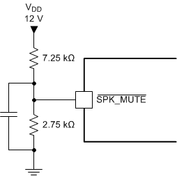 Figure 66. SPK_MUTE Used in External Undervoltage Error Protection
 Figure 67. SPK_MUTE Timing for External Undervoltage Error Protection
9.3.7.7 Internal Clock Error Notification (CLKE)
When a clock error is detected on the incoming data clock, the TAS5780M device switches to an internal oscillator and continues to the drive the DAC, while attenuating the data from the last known value. Once this process is complete, the DAC outputs will be hard muted to the ground and the class D PWM output will stop switching. The clock error can be monitored at B0-P0-R94 and R95. The clock error status bits are non-latching, except for MCLK halted B0-P0-R95-D[4] and CERF B0-P0-R95-D[0] which are cleared when read.
9.3.8 GPIO Port and Hardware Control Pins
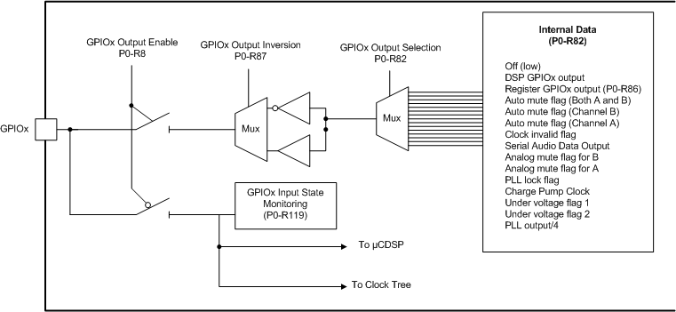 Figure 68. GPIO Port
9.3.9 I2C Communication Port
The TAS5780M device supports the I2C serial bus and the data transmission protocol for standard and fast mode as a slave device. Because the TAS5780M register map spans several books and pages, the user must select the correct book and page before writing individual register bits or bytes. Changing from book to book is accomplished by first changing to page 0x00 by writing 0x00 to register 0x00 and then writing the book number to register 0x7f of page 0. Changing from page to page is accomplished via register 0x00 on each page. The register value selects the register page, from 0 to 255.
9.3.9.1 Slave Address
Table 16. I2C Slave Address
| MSB | LSB | ||||||
| 1 | 0 | 0 | 1 | 1 | ADR2 | ADR1 | R/ W |
The TAS5780M device has 7 bits for the slave address. The first five bits (MSBs) of the slave address are factory preset to 10011 (0x9x). The next two bits of the address byte are the device select bits which can be user-defined by the ADR1 and ADR0 terminals. A maximum of four devices can be connected on the same bus at one time, which gives a range of 0x90, 0x92, 0x94 and 0x96, as detailed in Table 17. Each TAS5780M device responds when it receives the slave address.
Table 17. I2C Address Configuration via ADR0 and ADR1 Pins
| ADR1 | ADR0 | I2C SLAVE ADDRESS [R/W] |
|---|---|---|
| 0 | 0 | 0x90 |
| 0 | 1 | 0x92 |
| 1 | 0 | 0x94 |
| 1 | 1 | 0x96 |
9.3.9.2 Register Address Auto-Increment Mode
Auto-increment mode allows multiple sequential register locations to be written to or read back in a single operation, and is especially useful for block write and read operations. The TAS5780M device supports auto-increment mode automatically. Auto-increment stops at page boundaries.
9.3.9.3 Packet Protocol
A master device must control packet protocol, which consists of start condition, slave address, read/write bit, data if write or acknowledge if read, and stop condition. The TAS5780M device supports only slave receivers and slave transmitters.
 Figure 69. Packet Protocol
Table 18. Write Operation - Basic I2C Framework
| Transmitter | M | M | M | S | M | S | M | S | S | M | |
| Data Type | St | slave address | R/ | ACK | DATA | ACK | DATA | ACK | ACK | Sp |
Table 19. Read Operation - Basic I2C Framework
| Transmitter | M | M | M | S | S | M | S | M | M | M | |
| Data Type | St | slave address | R/ | ACK | DATA | ACK | DATA | ACK | NACK | Sp |
M = Master Device; S = Slave Device; St = Start Condition Sp = Stop Condition
9.3.9.4 Write Register
A master can write to any TAS5780M device registers using single or multiple accesses. The master sends a TAS5780M device slave address with a write bit, a register address, and the data. If auto-increment is enabled, the address is that of the starting register, followed by the data to be transferred. When the data is received properly, the index register is incremented by 1 automatically. When the index register reaches 0x7F, the next value is 0x0. Table 20 shows the write operation.
Table 20. Write Operation
| Transmitter | M | M | M | S | M | S | M | S | M | S | S | M | ||
| Data Type | St | slave addr | W | ACK | inc | reg addr | ACK | write data 1 | ACK | write data 2 | ACK | ACK | Sp | |
M = Master Device; S = Slave Device; St = Start Condition Sp = Stop Condition; W = Write; ACK = Acknowledge
9.3.9.5 Read Register
A master can read the TAS5780M device register. The value of the register address is stored in an indirect index register in advance. The master sends a TAS5780M device slave address with a read bit after storing the register address. Then the TAS5780M device transfers the data which the index register points to. When auto-increment is enabled, the index register is incremented by 1 automatically. When the index register reaches 0x7F, the next value is 0x0. Table 21 lists the read operation.
Table 21. Read Operation
| Transmitter | M | M | M | S | M | S | M | M | M | S | S | M | M | M | ||
| Data Type | St | slave addr | W | ACK | inc | reg addr | ACK | Sr | slave addr | R | ACK | data | ACK | NACK | Sp | |
M = Master Device; S = Slave Device; St = Start Condition; Sr = Repeated start condition; Sp = Stop Condition; W = Write; R = Read; NACK = Not acknowledge
9.3.9.6 DSP Book, Page, and Register Update
The DSP memory is arranged in books, pages, and registers. Each book has several pages and each page has several registers.
9.3.9.6.1 Book and Page Change
To change the book, the user must be on page 0x00. In register 0x7f on page 0x00 you can change the book. On page 0x00 of each book, register 0x7f is used to change the book. Register 0x00 of each page is used to change the page. To change a book first write 0x00 to register 0x00 to switch to page 0 then write the book number to register 0x7f on page 0. To change between pages in a book, simply write the page number to register 0x00.
9.3.9.6.2 Swap Flag
The swap flag is used to copy the audio coefficient from the host memory to the DSP memory. The swap flag feature is important to maintain the stability of the BQs. A BQ is a closed-loop system with 5 coefficients. To avoid instability in the BQ in an update transition between two different filters, update all five parameters within one audio sample. The internal swap flag insures all 5 coefficients for each filter are transferred from host memory to DSP memory occurs within an audio sample. The swap flag stays high until the full host buffer is transferred to DSP memory. Updates to the Host buffer should not be made while the swap flag is high.
All writes to book 0x8C from page 0x1B and register 0x58 through page 0x22 and register 0x1C require the swap flag. The swap flag is located in book 0x8C, page 0x01, and register 0x10 and must be set to 0x00 00 00 01 for a swap.
9.3.9.6.3 Example Use
The following is a sample script for using the DSP host memory to change the fine volume on the device on I2C slave address 0x90 to the default value of 0 dB:
w 90 00 00 #Go to page 0
w 90 7f 8C #Change the book to 0x8C
w 90 00 21 #Go to page 0x21
w 90 21 48 00 00 00 #Fine volume Left
w 90 21 4C 00 00 00 #Fine volume Right
#Run the swap flag for the DSP to work on the new coefficients
w 90 00 00 #Go to page 0
w 90 7f 8C #Change the book to 0x8C
w 90 00 01 #Go to page 0x01
w 90 10 00 00 00 01 #Swap flag
9.4 Device Functional Modes
Because the TAS5780M device is a highly configurable device, numerous modes of operation can exist for the device. For the sake of succinct documentation, these modes are divided into two modes:
- Fundamental operating modes
- Secondary usage modes
Fundamental operating modes are the primary modes of operation that affect the major operational characteristics of the device, which are the most basic configurations that are chosen to ensure compatibility with the intended application or the other components that interact with the device in the final system. Some examples of the operating modes are the communication protocol used by the control port, the output configuration of the amplifier, or the Master/Slave clocking configuration.
The fundamental operating modes are described starting in the Serial Audio Port Operating Modes section.
Secondary usage modes are best described as modes of operation that are used after the fundamental operating modes are chosen to fine tune how the device operates within a given system. These secondary usage modes can include selecting between left justified and right justified Serial Audio Port data formats, or enabling some slight gain/attenuation within the DAC path. Secondary usage modes are accomplished through manipulation of the registers and controls in the I2C control port. Those modes of operation are described in their respective register/bit descriptions and, to avoid redundancy, are not included in this section.
9.4.1 Serial Audio Port Operating Modes
The serial audio port in the TAS5780M device supports industry-standard audio data formats, including I2S, Time Division Multiplexing (TDM), Left-Justified (LJ), and Right-Justified (RJ) formats. To select the data format that will be used with the device, controls are provided on P0-R40. The timing diagrams for the serial audio port are shown in the Serial Audio Port Timing – Slave Mode section, and the data formats are shown in the Serial Audio Port – Data Formats and Bit Depths section.
9.4.2 Communication Port Operating Modes
The TAS5780M device is configured via an I2C communication port. The device does not support a hardware only mode of operation, nor Serial Peripheral Interface (SPI) communication. The I2C Communication Protocol is detailed in the I2C Communication Port section. The I2C timing requirements are described in the I2C Bus Timing – Standard and I2C Bus Timing – Fast sections.
9.4.3 Speaker Amplifier Operating Modes
The TAS5780M device can be used in two different amplifier configurations:
- Stereo Mode
- Mono Mode
9.4.3.1 Stereo Mode
The familiar stereo mode of operation uses the TAS5780M device to amplify two independent signals, which represent the left and right portions of a stereo signal. These amplified left and right audio signals are presented on differential output pairs shown as SPK_OUTA± and SPK_OUTB±. The routing of the audio data which is presented on the SPK_OUTxx outputs can be changed according to the Audio Process Flow which is used and the configuration of registers P0-R42-D[5:4] and P0-R42-D[1:0]. The familiar stereo mode of operation is shown in .
By default, the TAS5780M device is configured to output the Right frame of a I2S input on the Channel A output and the left frame on the Channel B output.
9.4.3.2 Mono Mode
The mono mode of operation is used to describe operation in which the two outputs of the device are placed in parallel with one another to increase the power sourcing capabilities of the audio output channel. This is also known as Parallel Bridge Tied Load (PBTL).
On the output side of the TAS5780M device, the summation of the devices can be done before the filter in a configuration called Pre-Filter PBTL. However, the two outputs may be required to merge together after the inductor portion of the output filter. Doing so does require two additional inductors, but allows smaller, less expensive inductors to be used because the current is divided between the two inductors. This process is called Post-Filter PBTL. Both variants of mono operation are shown in Figure 70 and Figure 71.
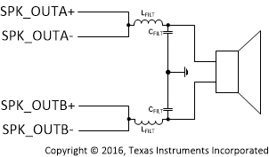 Figure 70. Pre-Filter PBTL
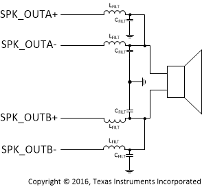 Figure 71. Post-Filter PBTL
On the input side of the TAS5780M device, the input signal to the mono amplifier can be selected from the any slot in a TDM stream or the left or right frame from an I2S, LJ, or RJ signal. The TAS5780M device can also be configured to amplify some mixture of two signals, as in the case of a subwoofer channel which mixes the left and right channel together and sends the mixture through a low-pass filter to create a mono, low-frequency signal.
The mono mode of operation is shown in the Mono (PBTL) Systems section.
9.4.3.3 Master and Slave Mode Clocking for Digital Serial Audio Port
The digital audio serial port in the TAS5780M device can be configured to receive clocks from another device as a serial audio slave device. The slave mode of operation is described in the Clock Slave Mode with SCLK PLL to Generate Internal Clocks (3-Wire PCM) section. If no system processor is available to provide the audio clocks, the TAS5780M device can be placed into Master Mode. In master mode, the TAS5780M device provides the clocks to the other audio devices in the system. For more details regarding the Master and Slave mode operation within the TAS5780M device, see the Serial Audio Port Operating Modes section.
9.5 Programming
9.5.1 Audio Processing Features
The TAS5780M device includes audio processing to optimize the audio performance of the audio system into which they are integrated. The TAS5780M device has 12 Biquad Filters for speaker response tuning, One dual band DPEQ to dynamically adjust the equalization curve that is applied to low-level signal and the curve that is applied to high level signals. A 2-band advanced DRC + AGL structure limits the output power of the amplifier for two regions while controlling the peaking that can occur in the crossover region during compression. A fine volume control is provided to finely adjust the output level of the amplifier based upon the system level considerations faced by the product development engineer.
The TAS5780M device has two signal monitoring options available, the level meter and the serial data out signal. The level meter monitors the signal level through an alpha filter and presents the signal in an I²C register. The level meter signal is taken before the 4x interpolation which occurs before the digital-to-analog conversion.
The SDOUT signal can be presented on any one of the GPIOx pins. Customarily, as is the case in all of the TI evaluation hardware for the TAS5780M device, GPIO2 is used.
The details of the audio processing flow, including the I²C control port registers associated with each block, are shown in .
 Figure 72. Fixed-Function Process Flow found in the TAS5780M
9.5.2 Processing Block Description
The processing block shown in the above is comprised of the following major blocks:
- Input scale and mixer
- Sample Rate Converter (SRC)
- Parametric Equalizers (PEQs)
- BQs Gain Scale
- Dynamic Parametric Equalizer (DPEQ)
- Two-Band Dynamic Ranger Control (DRC)
- Automatic Gain Limiter (AGL)
- Fine Volume
- Level Meter
- THD Management
9.5.2.1 Input Scale and Mixer
The input mixer can be used to mix the left and right channel input signals as shown in Figure 73. The input mixer has four coefficients, which control the mixing and gains of the input signals. When mixing and scaling the input signals, ensure that at maximum input level the input mixer outputs don't exceed 0 dBFS, which will overdrive the SRC inputs.
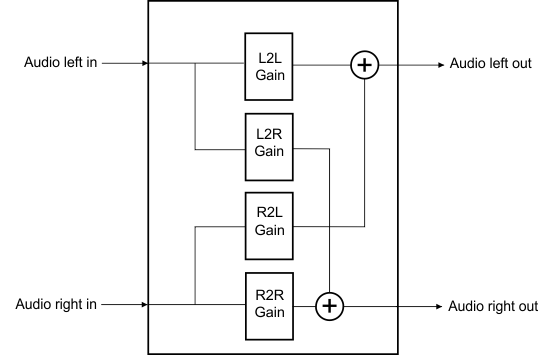 Figure 73. Input Scale and Mixer
9.5.2.1.1 Example
The following is a sample script for setting up the both left and right channels for (½L + ½R) or (L + R) / 2:
w 90 00 00 # Go to page 0
w 90 7f 8C #Change the book to 0x8C
w 90 00 21 #Go to page 0x21
w 90 50 00 40 26 E7 #Input mixer left in to left out gain
w 90 54 00 40 26 E7 #Input mixer right in to left out gain
w 90 58 00 40 26 E7 #Input mixer left in to right out gain
w 90 5C 00 40 26 E7 #Input mixer right in to right out gain
#Run the swap flag for the DSP to work on the new coefficients
w 90 00 00 #Go to page 0
w 90 7f 8C #Change the book to 0x8C
w 90 00 01 #Go to page 0x05
w 90 10 00 00 00 01 #Swap flag
9.5.2.2 Sample Rate Converter
The sample rate converter supports 32 kHz, 44.1 kHz, 48 kHz, 88.2 kHz and 96 kHz input sample rates. These input sample rates are converted to 88.2 or 96 kHz sample rate. The sample rate detection doesn’t distinguish between sample rates from 32 to 48 kHz. These sample rates are treated as 48 kHz by the sample rate converter. The detected sample rate can be read at book 0x78 page 0x0C register 0x5C. The input sample rate is 88.2 or 96 kHz at register 0x5C which reads 0x00 00 00 01. The input sample rate is 32 to 48 kHz at register 0x5C which reads 0x00 00 00 02. Input sample rate 32 kHz requires changing the interpolation setting from 2x to 3x by writing B0-P0-R37-D7 to 1. The device must be placed in standby mode for this change to take effect.
Table 22. Sample Rate Detection
| SAMPLING RATE (KHZ) | B0-P0-R91-D[6:4] |
|---|---|
| 8 | 001 |
| 16 | 010 |
| 32 – 48 | 011 |
| 88.2 – 96 | 100 |
Even though the sample rate converter supports 32 kHz, 44.1 kHz, 48 kHz, 88.2 kHz and 96 kHz input sample rates, the TAS5780M device supports all input sample rates shown in Table 22 in 1x interpolation mode, base rate processing.
The SRC input should not be overdriven. Making the maximum signal level into the SRC –0.5dBFs is recommended to prevent overdriving the SRC and causing audio artifacts. The input scale and mixer can be used to attenuate or boost the maximum input signal to –0.5dBFs. The processing block has several blocks after the SRC where the signal can be compensate for any gain attenuation done in the input mixer and scale block to prevent over driving the SRC.
9.5.2.3 Parametric Equalizers (PEQ)
The device supports 12 individual tuned PEQs for left channel and 12 individual tuned PEQs for the right channel. The PEQs are implemented using cascaded “direct form 1” BQs structures as shown in Figure 74.
 Figure 74. Cascaded BQ Structure

All BQ coefficients are normalized with a0 to insure that a0 is equal to 1. The structure requires 5 BQ coefficients as shown in Table x. Any BQ with coefficients greater than 1 undergoes gain scaling as described in BQ Gain Scale.
Table 23. BQ Coefficients Normalization
| BQ COEFFICIENT FOR TAS5780M | COEFFICIENT CALCULATION |
|---|---|
| B0_DSP | b0 / a0 |
| B1_DSP | b1 / (a0 × 2) |
| B2_DSP | b2 / a0 |
| A1_DSP | –a1 / (a0 × 2) |
| A2_DSP | –a2 / a0 |
9.5.2.4 BQ Gain Scale
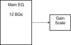 Figure 75. PEQs and BQs Gain Scale Block
The BQ coefficients format is as follows: The first BQ has B0 = 5.x, B1 = 6.x, B2 = 5.x, A1 = 2.x, and A2 = 1.x. The rest of the BQ have this format: B0 = 1.x, B1 = 2.x, B2 = 1.x, A1 = 2.x, and A2 = 1.x. This formatting maintains the highest possible resolution and noise performance. The 1.31 format restricts the ability to do high gains within the BQs and as a result requires gain compensation for the restriction. When generating BQ coefficients, ensure none of the BQ coefficients is greater than 1 by implementing gain compensation. The Gain compensation reduces the BQ coefficients gain to ensure all BQ coefficients are less than 1. The reduced gain is then reapplied in the subsequent gain scale block.
Gain compensation takes the maximum value of B0_DSP, B1_DSP, and B2_DSP after the BQ normalization shown in Table 23 is implemented. All the B coefficients are divided by maximum B coefficient value then multiplied by 0.999999999534339 (the nearest two’s complement 32-bit number to 1). The following calculations are done for each BQ in the PEQ block:


The calculations above insure all DSP BQ coefficients are in a 1.31 format. The reduced gains in the BQ 1.31 format is compensation for in the gain scale block. The following calculation is done for each channel.
The calculated k_BQ compensation value is then applied to the BQ gain scale in an 8.24 format. The BQ gain scale can also be used for volume control before the DRCs. The block can be considered as BQ gain scale and volume gain block. When the BQ gain scale block is used for volume control the coefficient value must be calculated as follows:

where
- Volume is in dB
The BQ gain scale coefficients are located in book 0x8C, page 0x1F register 0x58 for left and register 0x5C for right.
The Bypass EQ Mux allows the user to bypass all processing. The Bypass EQ mux is at Page 0x21, Register 0x64. The Gang Left / Right mux forces the left processing to be the same as the right processing. The Gang Left / Right Mux is located at Page 0x21, Register 0x68.
9.5.2.5 Dynamic Parametric Equalizer (DPEQ)
The dynamic parametric equalizer mixes the audio signals routed through two paths containing one BQ each based upon the signal level detected by the sense path, as shown in Figure 76. The sense path contains one BQ, which can be used to focus the DPEQ sensing on a specific frequency bandwidth. An alpha filter structure is used to sense the energy in the sense path and setting the dynamic mixing ratios.
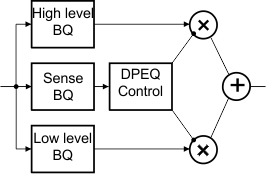 Figure 76. DPEQ Signal Path
The dynamic mixing is controlled by offset, gain, and alpha coefficients in a 1.31 format. The alpha coefficient controls the average time constant in ms of the signal data in the sense path. The offset and gain coefficients control the dynamic mixing thresholds shown in Figure 77.
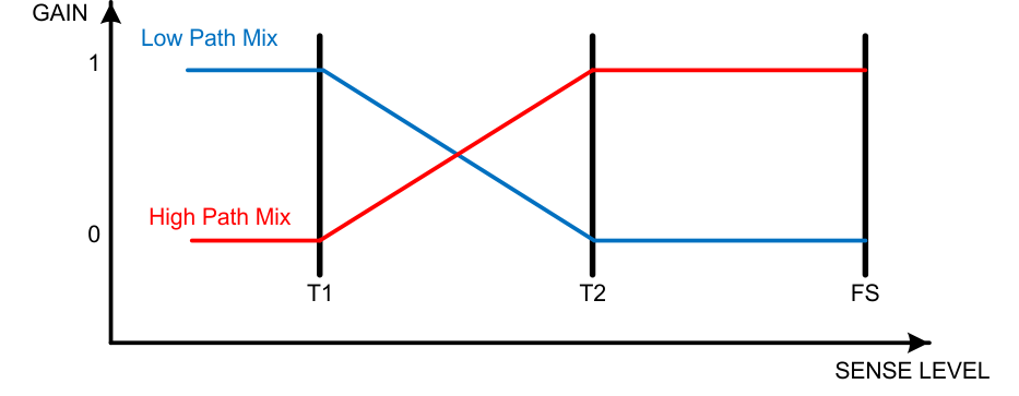 Figure 77. Dynamic Mixing
The offset, gain and alpha coefficients are calculated as follows:


where
- T2 ≥ –20 dB

where
- T2 < –20 dB


where
- T1 and T2 are in dB
- The time constant is in ms
The DPEQ control coefficients are located in book 0x8C, page0x20. Register 0x58 is alpha coefficient, register 0x5C is gain coefficient and register 0x60 is offset coefficient.
The high level path BQ, low level path BQ, and sense path BQ coefficients use a 1.31 format as shown in Table 25. The DPEQ BQs don't have a gain scale to compensate for any BQ gain reduction due to the requirements of the 1.31 format. During tuning, the reduced gain can be compensated by using the BQ gain scale or the DRC offset coefficient.
The DPEQ sense gain scale is located in the sensing path. The DPEQ sense gain scale can be used to shift the dynamic mixing thresholds by changing the signal level in the sensing path. A positive dB gain shifts the dynamic mixing thresholds down by the gain amount and a negative dB gain shifts the dynamic mixing thresholds up by the gain amount.
9.5.2.6 Two-Band Dynamic Range Control
The Dynamic Range Control (DRC) is a feed-forward mechanism that can be used to automatically control the audio signal amplitude or the dynamic range within specified limits. The dynamic range control is done by sensing the audio signal level using an estimate of the alpha filter energy then adjusting the gain based on the region and slope parameters that are defined. The Dynamic Range Control is shown in Figure 78.
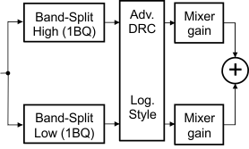 Figure 78. Dynamic Range Control
The DRCs have seven programmable transfer function parameters each: k0, k1, k2, T1, T2, OFF1, and OFF2. The T1 and T2 parameters specify thresholds or boundaries of the three compression or expansion regions in terms of input level. The Parameters k0, k1, and k2 define the gains or slopes of curves for each of the three regions. The parameters OFF1 and OFF2 specify the offset shift relative 1:1 transfer function curve at the thresholds T1 and T2 respectively shown in Figure 79.
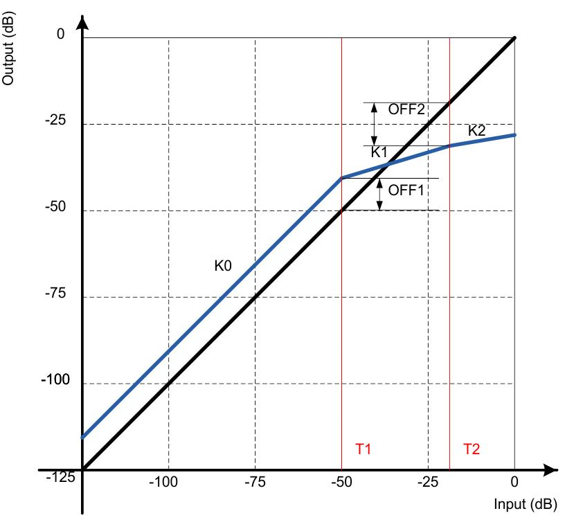 Figure 79. DRC Transfer Function Example Plot
The two-band dynamic range control is comprised of two DRCs that can be spilt into two bands using the BQ at the input of each band. The frequency where the two bands are spilt is referred to as the crossover frequency. The crossover frequency is the cut off frequency for the low pass filter used to create the low band and the cut off frequency for the high pass filter used to create the high band.
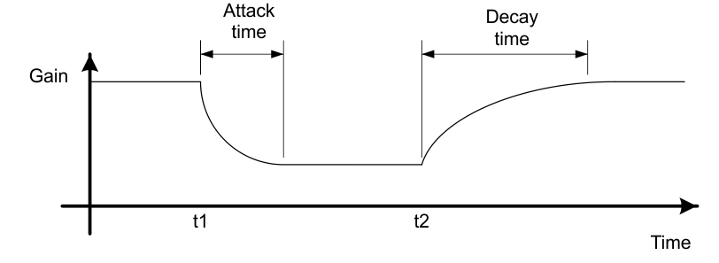 Figure 80. DRC Attack and Decay
The DRC in each band is equipped with individual energy, attack, and decay time constants. The DRC time constants control the transition time of changes and decisions in the DRC gain during compression or expansion. The energy, attack, and decay time constants affect the sensitivity level of the DRC. The shorter the time constant, the more aggressive the DRC response and vice versa.
9.5.2.7 Automatic Gain Limiter
The Automatic Gain Limiter (AGL) is a feedback mechanism that can be used to automatically control the audio signal amplitude or dynamic range within specified limits. The automatic gain limiting is done by sensing the audio signal level using an alpha filter energy structure shown in Figure 82 at the output of the AGL then adjusting the gain based on the whether the signal level is above or below the defined threshold. Three decisions made by the AGL are engage, disengage, or do nothing. The rate at which the AGL engages or disengages depends on the attack and release settings, respectively.
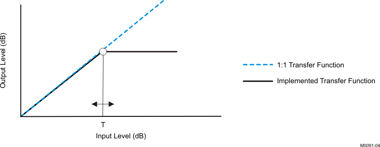 Figure 81. AGL Transfer Function Example Plot
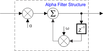 Figure 82. AGL Alpha Filter Structure
9.5.2.7.1 Softening Filter Alpha (AEA)
- AEA = 1 – e–1000 / (fs × User_AE)
- e ≈ 2.718281828
- Fs = sampling frequency
- User_AE = user input step size
9.5.2.7.2 Softening Filter Omega (AEO)
- AEO = 1 – AEA
9.5.2.7.3 Attack Rate
- Attack rate = 2 (AA + Release rate)
- AA = 1000 × User_Ad / Fs
- User_Ad = user input attack step size
9.5.2.7.4 Release Rate
- Release rate = 1000 × User_Rd / Fs
- User_Rd = user input release step size
NOTE
The release duration (User_Rd) should be longer than the attack duration (User_Ad).
9.5.2.7.5 Attack Threshold
- Attack Threshold = user input level in dB
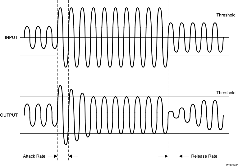 Figure 83. AGL Attack and Release
The Attack Threshold AGL coefficients are shown in .
9.5.2.8 Fine Volume
The fine volume block after the AGL can be used to provide additional fine volume steps from –192 dB to 6 dB in a 2.30 format. The Fine Coefficients are shown in .
9.5.2.9 THD Boost
A boost scalar and fine volume together can be used for clipping. The THD boost block allows the user to programmatically increase the THD by clipping at an operating point earlier than that defined by the supply rails.
9.5.2.10 Level Meter
The level meter uses an energy estimator with a programmable time constant to adjust the sensitivity level based on signal frequency and desired accuracy level. The level meter outputs of both left and right channels are written to a 32-bit sub address location in a 1.31 format as shown in . The BypassToLevelMeter Bit in Book 8C, Page 0x21, Register 0x70 can be used to switch the input to the Level Meter from the audio before processing to audio post-processing.
9.5.3 Other Processing Block Features
9.5.3.1 Number Format
The data processing path is 32 bits with 32-bit coefficients. The coefficients use the two’s complement digital number format.
Table 24. Two’s Complement Format
| BITS | TWO'S COMPLEMENT VALUE |
|---|---|
| 0111 1111 | 127 |
| 0111 1110 | 126 |
| 0000 0010 | 2 |
| 0000 0001 | 1 |
| 0000 0000 | 0 |
| 1111 1111 | –1 |
| 1111 1110 | –2 |
| 1000 0010 | –126 |
| 1000 0001 | –127 |
| 1000 0000 | –128 |
9.5.3.1.1 Coefficient Format Conversion
The device uses 32 bit two’s complement number formats. The calculated 4 byte register values are shown below in an 8 digit hex value.
Table 25. Sample Calculations for 1.31 Format
| dB | Linear | Decimal | Hex (1.31 Format) |
|---|---|---|---|
| 0 | 1 | 2147483648 | 7FFFFFFF |
| –6 | 0.5 | 1073741824 | 40000000 |
| –20 | 0.1 | 214748364 | 0CCCCCCC |
| x | L = 10(x/20) | D = 231 × L, D < 231
D = 231, D ≥ 231 |
Dec2Hex(D, 8)(1) |
Please note that for a 1.31 format the linear value cannot be greater than 1 or decimal value 232.
Table 26. Sample Calculations for B.A Format
| dB | Linear | Decimal | Hex (1.31 Format) |
|---|---|---|---|
| x | L = 10(x/20) | D = 2A × L, D < 2(B + A - 1)
D = 2(B + A - 1), D ≥ 2(B + A - 1) |
Dec2Hex(D, 8) |
9.5.4 Checksum
The TAS5780M device supports two different check sum schemes, a cyclic redundancy check (CRC) checksum and an Exclusive (XOR) checksum. Both checksums work on every register write, except for book switch register and page switching register, 0x7F and 0x00, respectively. Register reads do not change checksum, but writes to even nonexistent registers will change the checksum. Both checksums are 8-bit checksums and both are available together simultaneously. The checksums can be reset by writing a starting value (eg. 0x 00 00 00 00) to their respective 4-byte register locations.
9.5.4.1 Cyclic Redundancy Check (CRC) Checksum
The 8-bit CRC checksum used is the 0x7 polynomial (CRC-8-CCITT I.432.1; ATM HEC, ISDN HEC and cell delineation, (1 + x1 + x2 + x8). A major advantage of the CRC checksum is that it is input order sensitive.
The CRC supports all I2C transactions, excluding book and page switching. The CRC checksum is read from register 0x7E on any page of book 0x00 (B0_Page x_Reg 126). If the book isn’t Book 0, the CRC checksum is only valid on page 0x00 register 0x7E (Page 0_Reg 126). The CRC checksum can be reset by writing 0x00 00 00 00 to the same register locations where the CRC checksum is valid.
9.5.4.2 Exclusive or (XOR) Checksum
The Xor checksum is a simpler checksum scheme. It performs sequential XOR of each register byte write with the previous 8-bit checksum register value. XOR supports only YMEM, which is located in Book 0x8C and excludes page switching and all registers in Page 0x00 of Book 0x8C. XOR checksum is read from location register 0x7D on page 0x00 of book 0x8C (B140_Page 0_Reg 125). The XOR Checksum can be reset by writing 0x00 00 00 00 to the same register location where it is read.
Table 27. XOR Truth Table
| INPUT | OUTPUT | |
|---|---|---|
| A | B | |
| 0 | 0 | 0 |
| 0 | 1 | 1 |
| 1 | 0 | 1 |
| 1 | 1 | 0 |