ZHCSRU6F May 2002 – March 2023 SN65HVD05 , SN65HVD06 , SN65HVD07 , SN75HVD06 , SN75HVD07
PRODUCTION DATA
- 1 特性
- 2 应用
- 3 说明
- 4 Revision History
-
5 Specifications
- 5.1 Absolute Maximum Ratings
- 5.2 Recommended Operating Conditions
- 5.3 Thermal Information
- 5.4 Package Dissipation Ratings
- 5.5 Driver Electrical Characteristics
- 5.6 Driver Switching Characteristics
- 5.7 Receiver Electrical Characteristics
- 5.8 Receiver Switching Characteristics
- 5.9 Typical Characteristics
- 6 Function Tables
- 7 Equivalent Input and Output Schematic Diagrams
- 8 Application and Implementation
- 9 Device and Documentation Support
- 10Mechanical, Packaging, and Orderable Information
Parameter Measurement Information
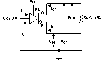
 Figure 6-1 Driver VOD Test Circuit and Voltage and Current Definitions
 Figure 6-2 Driver VOD With Common-Mode Loading Test Circuit
 Figure 6-3 Test Circuit and Definitions for the Driver Common-Mode Output Voltage
 Figure 6-4 Driver Switching Test Circuit and Voltage Waveforms
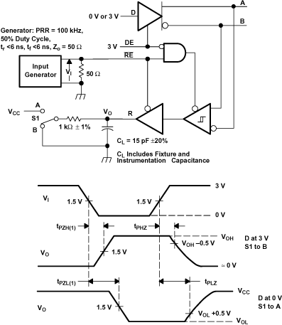
 Figure 6-5 Driver High-Level Enable and Disable Time Test Circuit and Voltage Waveforms
 Figure 6-6 Driver Low-Level Output Enable and Disable Time Test Circuit and Voltage Waveforms
 Figure 6-7 Receiver Voltage and Current Definitions
 Figure 6-8 Receiver Switching Test Circuit and Voltage Waveforms
 Figure 6-9 Receiver Enable and Disable Time Test Circuit and Voltage Waveforms With Drivers Enabled
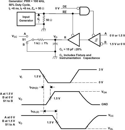
 Figure 6-10 Receiver Enable Time From Standby (Driver Disabled)
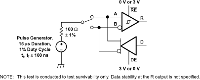
 Figure 6-11 Test Circuit, Transient Over Voltage Test