ZHCSK39C August   2019  – August 2020 OPA862

PRODUCTION DATA  

  1. 特性
  2. 应用
  3. 说明
  4. Revision History
  5. Pin Configuration and Functions
  6. Specifications
    1. 6.1 Absolute Maximum Ratings
    2. 6.2 ESD Ratings
    3. 6.3 Recommended Operating Conditions
    4. 6.4 Thermal Information
    5. 6.5 Electrical Characteristics: VS = ±2.5 V to ±5 V
    6. 6.6 Typical Characteristics: VS = ±5 V
    7. 6.7 Typical Characteristics: VS = ±2.5 V
    8. 6.8 Typical Characteristics: VS = 1.9 V, –1.4 V
    9. 6.9 Typical Characteristics: VS = 1.9 V, –1.4 V to ±5 V
  7. Detailed Description
    1. 7.1 Overview
    2. 7.2 Functional Block Diagram
    3. 7.3 Feature Description
      1. 7.3.1 Input and ESD Protection
      2. 7.3.2 Anti-Phase Reversal Protection
      3. 7.3.3 Precision and Low Noise
    4. 7.4 Device Functional Modes
      1. 7.4.1 Split-Supply Operation (±1.5 V to ±6.3 V)
      2. 7.4.2 Single-Supply Operation (3 V to 12.6 V)
  8. Application and Implementation
    1. 8.1 Application Information
      1. 8.1.1 Single-Ended-to-Differential Gain of 4 V/V
    2. 8.2 Typical Applications
      1. 8.2.1 Single-Ended to Differential with 2.5-V Output Common-Mode Voltage
        1. 8.2.1.1 Design Requirements
        2. 8.2.1.2 Detailed Design Procedure
        3. 8.2.1.3 Application Curves
      2. 8.2.2 Transimpedance Amplifier Configuration
        1. 8.2.2.1 Design Requirements
        2. 8.2.2.2 Detailed Design Procedure
        3. 8.2.2.3 Application Curves
      3. 8.2.3 DC Level-Shifting
  9. Power Supply Recommendations
  10. 10Layout
    1. 10.1 Layout Guidelines
    2. 10.2 Layout Examples
  11. 11Device and Documentation Support
    1. 11.1 Documentation Support
      1. 11.1.1 Related Documentation
    2. 11.2 Receiving Notification of Documentation Updates
    3. 11.3 支持资源
    4. 11.4 Trademarks
    5. 11.5 Electrostatic Discharge Caution
    6. 11.6 术语表
  12. 12Mechanical, Packaging, and Orderable Information

封装选项

机械数据 (封装 | 引脚)
散热焊盘机械数据 (封装 | 引脚)
订购信息

Typical Characteristics: VS = 1.9 V, –1.4 V to ±5 V

TA ≈ 25°C, A1 input common-mode voltage (VCM) = midsupply, VREF = midsupply, RF (connected between
VOUT+ and VFB) = 0 Ω, RG = open, differential gain (G) = 2 V/V, RL (differential load) = 2 kΩ, and RREF = 0 Ω (unless otherwise noted).
GUID-9FCE8070-4BC8-4D44-94D0-9CA9E4F69A4F-low.gif
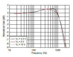
VIN = 10 mVPP, VREF = 0 V, measured at VOUT+
Figure 6-35 A1 Small-Signal Frequency Response
GUID-098B87D6-A03C-4F86-8206-17791B1BCC14-low.gif
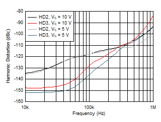
VOD = 10 VPP for 10-V supply, VOD = 5 VPP for 5-V supply
Figure 6-37 Harmonic Distortion vs Frequency
GUID-42A28684-22D3-47A4-83FF-BEA8958E1A56-low.gif
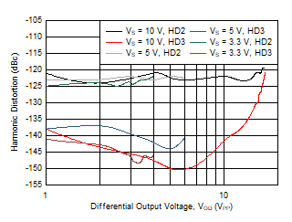
Frequency = 50 kHz
Figure 6-39 Harmonic Distortion vs Differential Output Voltage
GUID-D4B460FE-4CEE-4850-BDBE-26D0945FCDE7-low.gif
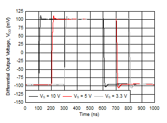
VOD = 200 mVPP
Figure 6-41 Small-Signal Step Response
GUID-DB5AED4F-0BDB-4B3E-AD78-C6A9625B0B39-low.gif
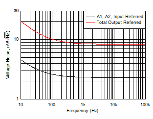
1/f corner (A1, A2) = 30 Hz, 1/f corner (output) = 49 Hz
Figure 6-43 Voltage Noise Density vs Frequency
GUID-EB49525A-5ADD-4ADE-8691-BC804E3DECB6-low.gif
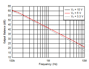
Figure 6-45 Output Balance vs Frequency
GUID-778CAD5A-DA9E-4111-9D27-ED68379BD440-low.gif
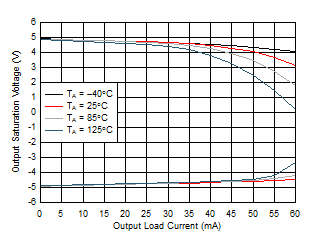
VS = 10 V, single-ended output voltage and load current for A1 and A2
Figure 6-47 Output Saturation Voltage vs Output Load Current
GUID-2E8E7439-517B-4329-B6B8-9CDA80EE732A-low.gif
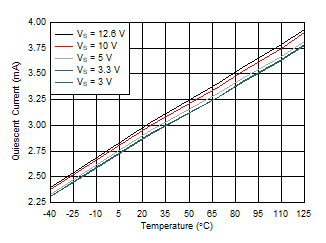
Figure 6-49 Quiescent Current vs Temperature
GUID-187334A0-120C-4368-B2B1-50786E0CFB7E-low.gif
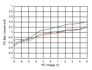
VS = 10 V
Figure 6-51 Power-Down Bias Current vs Power-Down Voltage
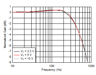
GUID-BAE2317F-1D15-4D80-99A4-83783C47D5B1-low.gif
VIN = 0 V, VREF = 20 mVPP, measured at VOUT–
Figure 6-36 VREF Small-Signal Frequency Response
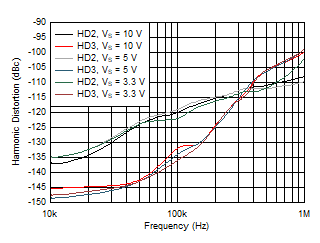
GUID-55922692-38D8-482B-AADB-DEB0D52ACA30-low.gif
VOD = 2 VPP
Figure 6-38 Harmonic Distortion vs Frequency
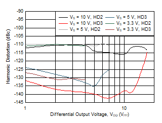
GUID-13073807-E1E4-4C57-926C-470F068EBA8E-low.gif
Frequency = 50 kHz, G = –2 V/V
Figure 6-40 Harmonic Distortion vs Differential Output Voltage
GUID-EB5D67E6-D62B-4F96-8275-6F182901B739-low.gif
Figure 6-42 Large-Signal Step Response
GUID-FEEE602A-8810-4197-B65A-4E19CC8B9966-low.gif
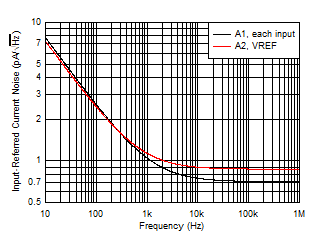
1/f corner (A1) = 1.2 kHz, 1/f corner (A2) = 700 Hz
Figure 6-44 Current Noise Density vs Frequency
GUID-0A5392EA-E2EC-49CA-AC96-CF94599B3F37-low.gif
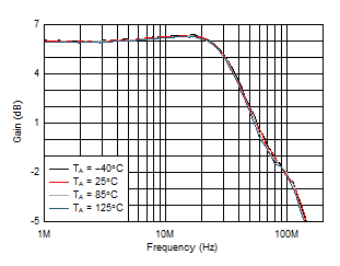
VS = 5 V, VOD = 20 mVPP
Figure 6-46 Small-Signal Frequency Response vs Temperature
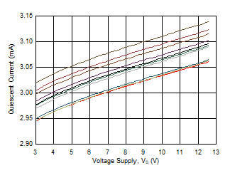
GUID-6A548098-4BC5-454C-AA5E-BA22AE0A4D9C-low.gif
Figure 6-48 Quiescent Current vs Voltage Supply
GUID-8AE6C319-FDD5-4BFD-A508-EC872FD8C6FC-low.gif
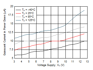
Figure 6-50 Power-Down Quiescent Current vs Voltage Supply
GUID-4B7F53C4-846A-47D6-B04B-8CB6B5A4C62B-low.gif
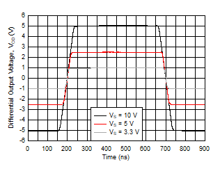
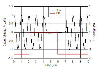
VS = 5 V
Figure 6-52 Turnon and Turnoff Timing