ZHCSBC7E JULY 2013 – December 2019 LMZ31710
PRODUCTION DATA.
- 1 特性
- 2 应用
- 3 说明
- 4 修订历史记录
- 5 Pin Configuration and Functions
- 6 Specifications
-
7 Detailed Description
- 7.1 Overview
- 7.2 Functional Block Diagram
- 7.3
Feature Description
- 7.3.1 VIN and PVIN Input Voltage
- 7.3.2 3.3-V PVIN Operation
- 7.3.3 Adjusting the Output Voltage (0.6 V to 5.5 V)
- 7.3.4 Capacitor Recommendations For the LMZ31710 Power Supply
- 7.3.5 Transient Response
- 7.3.6 Power Good (PWRGD)
- 7.3.7 Light Load Efficiency (LLE)
- 7.3.8 SYNC_OUT
- 7.3.9 Parallel Operation
- 7.3.10 Power-Up Characteristics
- 7.3.11 Pre-Biased Start-Up
- 7.3.12 Remote Sense
- 7.3.13 Thermal Shutdown
- 7.3.14 Output On/Off Inhibit (INH)
- 7.3.15 Slow Start (SS/TR)
- 7.3.16 Overcurrent Protection
- 7.3.17 Synchronization (CLK)
- 7.3.18 Sequencing (SS/TR)
- 7.4 Device Functional Modes
- 8 Application and Implementation
- 9 Power Supply Recommendations
- 10Layout
- 11器件和文档支持
- 12机械、封装和可订购信息
7.3.14 Output On/Off Inhibit (INH)
The INH pin provides electrical on/off control of the device. Once the INH pin voltage exceeds the threshold voltage, the device starts operation. If the INH pin voltage is pulled below the threshold voltage, the regulator stops switching and enters low quiescent current state. The INH pin has an internal pull-up current source, allowing the user to float the INH pin for enabling the device.
If an application requires controlling the INH pin, use an open drain/collector device, or a suitable logic gate to interface with the pin. Using a voltage supervisor to control the INH pin allows control of the turn-on and turn-off of the device as opposed to relying on the ramp up or down if the input voltage source.
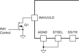
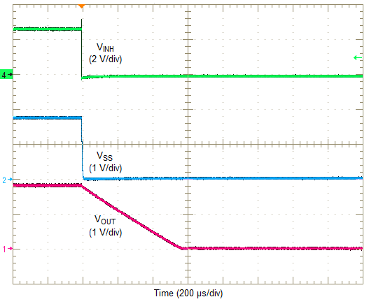
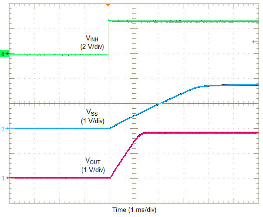
Figure 26 shows the typical application of the inhibit function. Turning Q1 on applies a low voltage to the inhibit control (INH) pin and disables the output of the supply, shown in Figure 27. If Q1 is turned off, the supply executes a soft-start power-up sequence, as shown in Figure 28. A regulated output voltage is produced within 2 ms. The waveforms were measured with a 5-A constant current load.
 Figure 26. Typical Inhibit Control
  Figure 27. Inhibit Turn Off
  Figure 28. Inhibit Turn On