ZHCSDM5G March 2012 – December 2014 LMK00105
PRODUCTION DATA.
- 1 特性
- 2 应用
- 3 说明
- 4 修订历史
- 5 Pin Configuration and Diagrams
- 6 Specifications
- 7 Detailed Description
- 8 Application and Implementation
- 9 Power Supply Recommendations
- 10Layout
- 11器件和文档支持
- 12机械、封装和可订购信息
9 Power Supply Recommendations
9.1 Power Supply Filtering
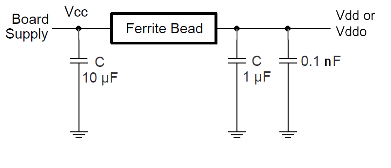
It is recommended, but not required, to insert a ferrite bead between the board power supply and the chip power supply to isolate the high-frequency switching noises generated by the clock driver, preventing them from leaking into the board supply. Choosing an appropriate ferrite bead with very low DC resistance is important, because it is imperative to provide adequate isolation between the board supply and the chip supply. It is also imperative to maintain a voltage at the supply terminals that is greater than the minimum voltage required for proper operation.
 Figure 21. Power-Supply Decoupling
9.2 Power Supply Ripple Rejection
In practical system applications, power supply noise (ripple) can be generated from switching power supplies, digital ASICs or FPGAs, etc. While power supply bypassing will help filter out some of this noise, it is important to understand the effect of power supply ripple on the device performance. When a single-tone sinusoidal signal is applied to the power supply of a clock distribution device, such as LMK00105, it can produce narrow-band phase modulation as well as amplitude modulation on the clock output (carrier). In the singleside band phase noise spectrum, the ripple-induced phase modulation appears as a phase spur level relative to the carrier (measured in dBc).
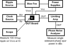
For the LMK00105, power supply ripple rejection (PSRR), was measured as the single-sideband phase spur level (in dBc) modulated onto the clock output when a ripple signal was injected onto the Vddo supply. The PSRR test setup is shown in Figure 22.
 Figure 22. PSRR Test Setup
A signal generator was used to inject a sinusoidal signal onto the Vddo supply of the DUT board, and the peak-to-peak ripple amplitude was measured at the Vddo pins of the device. A limiting amplifier was used to remove amplitude modulation on the differential output clock and convert it to a single-ended signal for the phase noise analyzer. The phase spur level measurements were taken for clock frequencies of 100 MHz under the following power supply ripple conditions:
- Ripple amplitude: 100 mVpp on Vddo = 2.5 V
- Ripple frequency: 100 kHz
Assuming no amplitude modulation effects and small index modulation, the peak-to-peak deterministic jitter (DJ) can be calculated using the measured single-sideband phase spur level (PSRR) as follows:
9.3 Power Supply Bypassing
The Vdd and Vddo power supplies should have a high frequency bypass capacitor, such as 100 pF, placed very close to each supply pin. Placing the bypass capacitors on the same layer as the LMK00105 improves input sensitivity and performance. All bypass and decoupling capacitors should have short connections to the supply and ground plane through a short trace or via to minimize series inductance.