ZHCSJN1C September   2000  – September 2022 INA118

PRODUCTION DATA  

  1. 特性
  2. 应用
  3. 说明
  4. Revision History
  5. Device Comparison Table
  6. Pin Configuration and Functions
  7. Specifications
    1. 7.1 绝对最大额定值
    2. 7.2 ESD Ratings
    3. 7.3 Recommended Operating Conditions
    4. 7.4 Thermal Information
    5. 7.5 Electrical Characteristics
    6. 7.6 Typical Characteristics
  8. Detailed Description
    1. 8.1 Overview
    2. 8.2 Functional Block Diagram
    3. 8.3 Feature Description
    4. 8.4 Device Functional Modes
      1. 8.4.1 Noise Performance
      2. 8.4.2 Input Common-Mode Range
      3. 8.4.3 Input Protection
  9. 应用和实现
    1. 9.1 应用信息
    2. 9.2 Typical Application
      1. 9.2.1 Design Requirements
      2. 9.2.2 Detailed Design Procedure
        1. 9.2.2.1 Setting the Gain
        2. 9.2.2.2 Dynamic Performance
        3. 9.2.2.3 Offset Trimming
        4. 9.2.2.4 Input Bias Current Return Path
      3. 9.2.3 应用曲线
    3. 9.3 Power Supply Recommendations
      1. 9.3.1 Low-Voltage Operation
      2. 9.3.2 Single-Supply Operation
    4. 9.4 Layout
      1. 9.4.1 Layout Guidelines
      2. 9.4.2 Layout Example
  10. 10Device and Documentation Support
    1. 10.1 Device Support
      1. 10.1.1 Development Support
    2. 10.2 接收文档更新通知
    3. 10.3 支持资源
    4. 10.4 Trademarks
    5. 10.5 Electrostatic Discharge Caution
    6. 10.6 术语表
  11. 11Mechanical, Packaging, and Orderable Information

封装选项

机械数据 (封装 | 引脚)
散热焊盘机械数据 (封装 | 引脚)
订购信息

Typical Characteristics

at TA = 25°C, VS = ±15 V (unless otherwise noted)
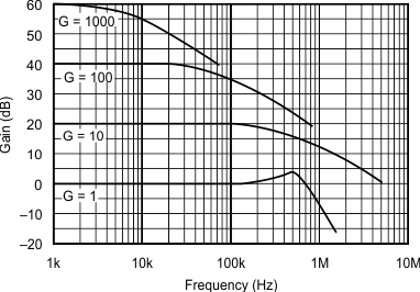
GUID-57F690DE-4DE5-45C5-BD6D-89EA98A9E060-low.gif
 
Figure 7-1 Gain vs Frequency
  VS = ±15 V
Figure 7-3 Input Common-Mode Range vs Output Voltage
  VS = 5 V
G = 1
Figure 7-5 Input Common-Mode Range vs Output Voltage
 
Figure 7-7 Positive Power Supply Rejection vs Frequency
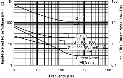
GUID-DDB7CE71-C870-4D2B-9F7E-93FD906CADCF-low.gif
 
Figure 7-9 Input-Referred Noise Voltage vs Frequency
 
Figure 7-11 Quiescent Current and Slew Rate vs Temperature
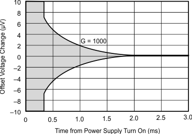
GUID-209AE87D-188F-4BD9-B17B-3E95C842BF0F-low.gif
 
Figure 7-13 Offset Voltage vs Warm-Up Time
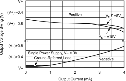
GUID-31DDE614-B5D0-440F-8CAA-1D9339C323FB-low.gif
 
Figure 7-15 Output Voltage Swing vs Output Current
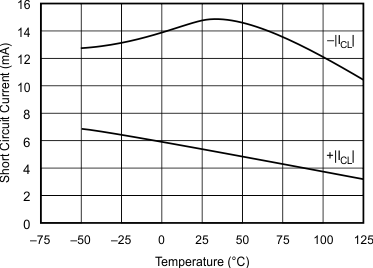
GUID-710A09E3-5839-4886-A449-3D0B44DAD53E-low.gif
 
Figure 7-17 Output Current Limit vs Temperature
 
Figure 7-19 THD + N vs Frequency
GUID-D76990A9-8B71-4D80-AFC2-594CC26A75B4-low.gif
 
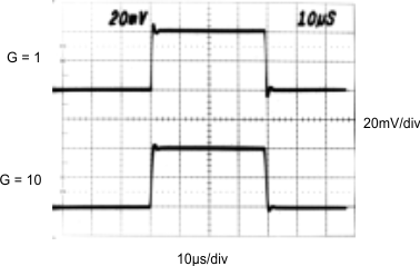
Figure 7-21 Small-Signal Response
GUID-02EC24EC-05E6-4FFC-B268-5357CCBD54A1-low.gif
 
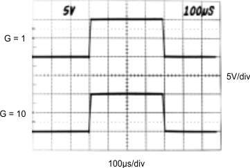
Figure 7-23 Large-Signal Response
GUID-A044529F-C380-45B2-859D-ABC40436F88D-low.gif
 
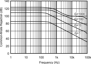
Figure 7-2 Common-Mode Rejection vs Frequency
  VS = ±5 V
Figure 7-4 Input Common-Mode Range vs Output Voltage
  VS = 5 V
G = 100
Figure 7-6 Input Common-Mode Range vs Output Voltage
 
Figure 7-8 Negative Power Supply Rejection vs Frequency
GUID-ADA75195-B5B6-40AD-96F4-1B1AF905767E-low.gif
 
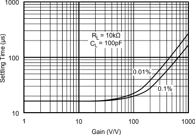
Figure 7-10 Settling Time vs Gain
 
Figure 7-12 Input Bias Current vs Input Overload Voltage
GUID-3E0080EB-336D-4129-832A-8B73A523A3B3-low.gif
 
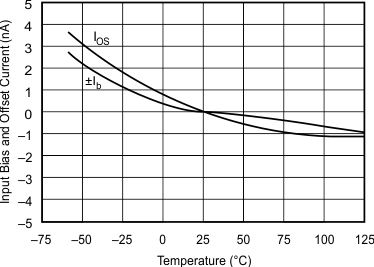
Figure 7-14 Input Bias and Offset Current vs Temperature
GUID-623AA8F0-54FD-43C9-81C0-E9FBED6E8C74-low.gif
 
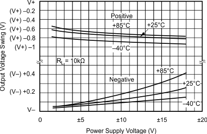
Figure 7-16 Output Voltage Swing vs Power Supply Voltage
 
Figure 7-18 Maximum Output Swing vs Frequency
  G = 1000
Figure 7-20 Input-Referred Noise, 0.1 Hz to 10 Hz
GUID-59A33FC7-5908-42D7-853B-E6B1B65F4593-low.gif
 
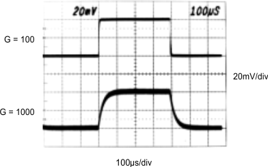
Figure 7-22 Small-Signal Response
GUID-F077D4AD-8424-4756-AA8E-BBA111E68A64-low.gif
 
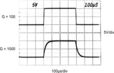
Figure 7-24 Large-Signal Response