ZHCSEN7D October 2014 – February 2022 DS90UB948-Q1
PRODUCTION DATA
- 1 特性
- 2 应用
- 3 说明
- 4 Revision History
- 5 Pin Configuration and Functions
-
6 Specifications
- 6.1 Absolute Maximum Ratings
- 6.2 ESD Ratings
- 6.3 Recommended Operating Conditions
- 6.4 Thermal Information
- 6.5 DC Electrical Characteristics
- 6.6 AC Electrical Characteristics
- 6.7 Timing Requirements for the Serial Control Bus
- 6.8 Switching Characteristics
- 6.9 Timing Diagrams and Test Circuits
- 6.10 Typical Characteristics
-
7 Detailed Description
- 7.1 Overview
- 7.2 Functional Block Diagram
- 7.3
Feature Description
- 7.3.1 High-Speed Forward Channel Data Transfer
- 7.3.2 Low-Speed Back Channel Data Transfer
- 7.3.3 FPD-Link III Port Register Access
- 7.3.4 Oscillator Output
- 7.3.5 Clock and Output Status
- 7.3.6 LVCMOS VDDIO Option
- 7.3.7 Power Down (PDB)
- 7.3.8 Interrupt Pin — Functional Description and Usage (INTB_IN)
- 7.3.9 General-Purpose I/O (GPIO)
- 7.3.10 SPI Communication
- 7.3.11 Backward Compatibility
- 7.3.12 Adaptive Equalizer
- 7.3.13 I2S Audio Interface
- 7.3.14 Repeater
- 7.3.15 Built-In Self Test (BIST)
- 7.3.16 Internal Pattern Generation
- 7.4
Device Functional Modes
- 7.4.1
Configuration Select MODE_SEL[1:0]
- 7.4.1.1 1-Lane FPD-Link III Input, Single Link OpenLDI Output
- 7.4.1.2 1-Lane FPD-Link III Input, Dual Link OpenLDI Output
- 7.4.1.3 2-Lane FPD-Link III Input, Dual Link OpenLDI Output
- 7.4.1.4 2-Lane FPD-Link III Input, Single Link OpenLDI Output
- 7.4.1.5 1-Lane FPD-Link III Input, Single Link OpenLDI Output (Replicate)
- 7.4.2 MODE_SEL[1:0]
- 7.4.3 OpenLDI Output Frame and Color Bit Mapping Select
- 7.4.1
Configuration Select MODE_SEL[1:0]
- 7.5 Image Enhancement Features
- 7.6
Programming
- 7.6.1 Serial Control Bus
- 7.6.2 Multi-Controller Arbitration Support
- 7.6.3 I2C Restrictions on Multi-Controller Operation
- 7.6.4 Multi-Controller Access to Device Registers for Newer FPD-Link III Devices
- 7.6.5 Multi-Controller Access to Device Registers for Older FPD-Link III Devices
- 7.6.6 Restrictions on Control Channel Direction for Multi-Controller Operation
- 7.7 Register Maps
- 8 Application and Implementation
- 9 Power Supply Recommendations
- 10Layout
- 11Device and Documentation Support
- 12Mechanical, Packaging, and Orderable Information
7.4.2 MODE_SEL[1:0]
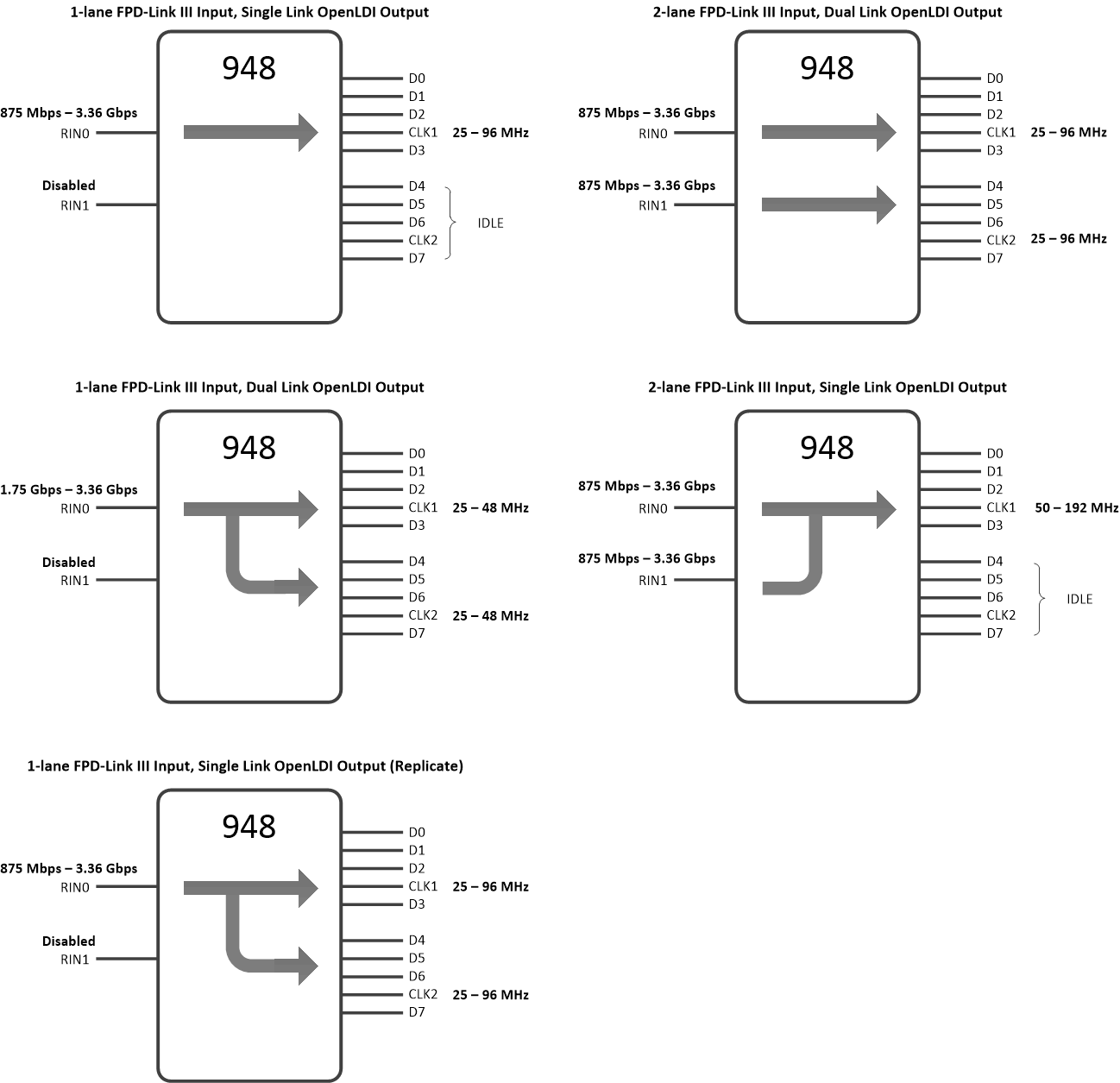
Possible configurations are shown in Figure 7-15. These are described above (Section 7.4.1).
 Figure 7-15 Data-Path
Configurations
Figure 7-15 Data-Path
Configurations![MODE_SEL[1:0] Connection Diagram GUID-E9DF3F71-F790-4331-B469-0F9DCE25D231-low.gif](/ods/images/ZHCSEN7D/GUID-E9DF3F71-F790-4331-B469-0F9DCE25D231-low.gif) Figure 7-16 MODE_SEL[1:0] Connection Diagram
Figure 7-16 MODE_SEL[1:0] Connection DiagramTable 7-8 Configuration Select (MODE_SEL0)
| NO. | VMODE VOLTAGE | VMODE TARGET VOLTAGE | SUGGESTED STRAP RESISTORS (1% tolerance) | MAP_SEL | OUTPUT_MODE [1:0] | OUTPUT MODE | |
|---|---|---|---|---|---|---|---|
| V (TYP) | VDD33 = 3.3 V | R1 (kΩ) | R2 (kΩ) | ||||
| 0 | 0 | 0 | Open | 10 | 0 | 00 | Dual OLDI output |
| 1 | 0.169 x V(VDD33) | 0.559 | 73.2 | 15 | 0 | 01 | Dual SWAP output |
| 2 | 0.230 x V(VDD33) | 0.757 | 66.5 | 20 | 0 | 10 | Single OLDI output |
| 3 | 0.295 x V(VDD33) | 0.974 | 59 | 24.9 | 0 | 11 | Replicate |
| 4 | 0.376 x V(VDD33) | 1.241 | 49.9 | 30.1 | 1 | 00 | Dual OLDI output |
| 5 | 0.466 x V(VDD33) | 1.538 | 46.4 | 40.2 | 1 | 01 | Dual SWAP output |
| 6 | 0.556 x V(VDD33) | 1.835 | 40.2 | 49.9 | 1 | 10 | Single OLDI output |
| 7 | 0.801 x V(VDD33) | 2.642 | 18.7 | 75 | 1 | 11 | Replicate |
Table 7-9 Configuration Select (MODE_SEL1)
| NO. | VMODE VOLTAGE | VMODE TARGET VOLTAGE | SUGGESTED STRAP RESISTORS (1% tolerance) | REPEATER | MODE | HIGH-SPEED BACK CHANNEL | INPUT MODE | |
|---|---|---|---|---|---|---|---|---|
| V (TYP) | VDD33 = 3.3 V | R1 (kΩ) | R2 (kΩ) | |||||
| 0 | 0 | 0 | Open | 10 | 0 | 00 | 5 Mbps | STP |
| 1 | 0.169 x V(VDD33) | 0.559 | 73.2 | 15 | 0 | 01 | 5 Mbps | Coax |
| 2 | 0.230 x V(VDD33) | 0.757 | 66.5 | 20 | 0 | 10 | 20 Mbps | STP |
| 3 | 0.295 x V(VDD33) | 0.974 | 59 | 24.9 | 0 | 11 | 20 Mbps | Coax |
| 4 | 0.376 x V(VDD33) | 1.241 | 49.9 | 30.1 | 1 | 00 | 5 Mbps | STP |
| 5 | 0.466 x V(VDD33) | 1.538 | 46.4 | 40.2 | 1 | 01 | 5 Mbps | Coax |
| 6 | 0.556 x V(VDD33) | 1.835 | 40.2 | 49.9 | 1 | 10 | 20 Mbps | STP |
| 7 | 0.801 x V(VDD33) | 2.642 | 18.7 | 75 | 1 | 11 | 20 Mbps | Coax |