ZHCSEN7D October 2014 – February 2022 DS90UB948-Q1
PRODUCTION DATA
- 1 特性
- 2 应用
- 3 说明
- 4 Revision History
- 5 Pin Configuration and Functions
-
6 Specifications
- 6.1 Absolute Maximum Ratings
- 6.2 ESD Ratings
- 6.3 Recommended Operating Conditions
- 6.4 Thermal Information
- 6.5 DC Electrical Characteristics
- 6.6 AC Electrical Characteristics
- 6.7 Timing Requirements for the Serial Control Bus
- 6.8 Switching Characteristics
- 6.9 Timing Diagrams and Test Circuits
- 6.10 Typical Characteristics
-
7 Detailed Description
- 7.1 Overview
- 7.2 Functional Block Diagram
- 7.3
Feature Description
- 7.3.1 High-Speed Forward Channel Data Transfer
- 7.3.2 Low-Speed Back Channel Data Transfer
- 7.3.3 FPD-Link III Port Register Access
- 7.3.4 Oscillator Output
- 7.3.5 Clock and Output Status
- 7.3.6 LVCMOS VDDIO Option
- 7.3.7 Power Down (PDB)
- 7.3.8 Interrupt Pin — Functional Description and Usage (INTB_IN)
- 7.3.9 General-Purpose I/O (GPIO)
- 7.3.10 SPI Communication
- 7.3.11 Backward Compatibility
- 7.3.12 Adaptive Equalizer
- 7.3.13 I2S Audio Interface
- 7.3.14 Repeater
- 7.3.15 Built-In Self Test (BIST)
- 7.3.16 Internal Pattern Generation
- 7.4
Device Functional Modes
- 7.4.1
Configuration Select MODE_SEL[1:0]
- 7.4.1.1 1-Lane FPD-Link III Input, Single Link OpenLDI Output
- 7.4.1.2 1-Lane FPD-Link III Input, Dual Link OpenLDI Output
- 7.4.1.3 2-Lane FPD-Link III Input, Dual Link OpenLDI Output
- 7.4.1.4 2-Lane FPD-Link III Input, Single Link OpenLDI Output
- 7.4.1.5 1-Lane FPD-Link III Input, Single Link OpenLDI Output (Replicate)
- 7.4.2 MODE_SEL[1:0]
- 7.4.3 OpenLDI Output Frame and Color Bit Mapping Select
- 7.4.1
Configuration Select MODE_SEL[1:0]
- 7.5 Image Enhancement Features
- 7.6
Programming
- 7.6.1 Serial Control Bus
- 7.6.2 Multi-Controller Arbitration Support
- 7.6.3 I2C Restrictions on Multi-Controller Operation
- 7.6.4 Multi-Controller Access to Device Registers for Newer FPD-Link III Devices
- 7.6.5 Multi-Controller Access to Device Registers for Older FPD-Link III Devices
- 7.6.6 Restrictions on Control Channel Direction for Multi-Controller Operation
- 7.7 Register Maps
- 8 Application and Implementation
- 9 Power Supply Recommendations
- 10Layout
- 11Device and Documentation Support
- 12Mechanical, Packaging, and Orderable Information
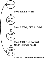
7.3.15.1.1 Sample BIST Sequence
Note: Before BIST can be enabled, D_GPIO0 (pin 19) must be strapped HIGH and D_GPIO[3:1] (pins 16, 17, and 18) must be strapped LOW.
- BIST Mode is enabled through the BISTEN pin of deserializer. The desired clock source is selected through the deserializer BISTC pin.
- The serializer is awakened through the back channel if it is not already on. An all-zeros pattern is balanced, scrambled, randomized, and sent through the FPD-Link III interface to the deserializer. Once the serializer and the deserializer are in BIST mode and the deserializer acquires LOCK, the PASS pin of the deserializer goes high and BIST starts checking the data stream. If an error in the payload (1 to 35) is detected, the PASS pin switches low for one half of the clock period. During the BIST test, the PASS output can be monitored and counted to determine the payload error rate per 35 bits.
- To stop BIST mode, set the BISTEN pin LOW. BIST duration is user-controlled and may be of any length.
The link returns to normal operation after the deserializer BISTEN pin is low. Figure 7-14 shows the waveform diagram of a typical BIST test for two cases. Case 1 is error-free, and Case 2 shows one with multiple errors. In most cases, it is difficult to generate errors due to the robustness of the link (differential data transmission, and so forth). Errors may be introduced by greatly extending the cable length, faulting the interconnect medium, or reducing signal condition enhancements (Rx equalization).
 Figure 7-13 BIST Mode Flow Diagram