ZHCSHZ0A April   2018  – July 2018 DRV8306

PRODUCTION DATA.  

  1. 特性
  2. 应用
  3. 说明
    1.     简化原理图
  4. 修订历史记录
  5. Pin Configuration and Functions
    1.     Pin Functions
  6. Specifications
    1. 6.1 Absolute Maximum Ratings
    2. 6.2 ESD Ratings
    3. 6.3 Recommended Operating Conditions
    4. 6.4 Thermal Information
    5. 6.5 Electrical Characteristics
    6. 6.6 Typical Characteristics
  7. Detailed Description
    1. 7.1 Overview
    2. 7.2 Functional Block Diagram
    3. 7.3 Feature Description
      1. 7.3.1 Three Phase Smart Gate Drivers
        1. 7.3.1.1 PWM Control Mode (1x PWM Mode)
        2. 7.3.1.2 Hardware Interface Mode
        3. 7.3.1.3 Gate Driver Voltage Supplies
        4. 7.3.1.4 Smart Gate Drive Architecture
          1. 7.3.1.4.1 IDRIVE: MOSFET Slew-Rate Control
          2. 7.3.1.4.2 TDRIVE: MOSFET Gate Drive Control
          3. 7.3.1.4.3 Gate Drive Clamp
          4. 7.3.1.4.4 Propagation Delay
          5. 7.3.1.4.5 MOSFET VDS Monitors
          6. 7.3.1.4.6 VDRAIN Sense Pin
      2. 7.3.2 DVDD Linear Voltage Regulator
      3. 7.3.3 Pulse-by-Pulse Current Limit
      4. 7.3.4 Hall Comparators
      5. 7.3.5 FGOUT Signal
      6. 7.3.6 Pin Diagrams
      7. 7.3.7 Gate-Driver Protective Circuits
        1. 7.3.7.1 VM Supply Undervoltage Lockout (UVLO)
        2. 7.3.7.2 VCP Charge-Pump Undervoltage Lockout (CPUV)
        3. 7.3.7.3 MOSFET VDS Overcurrent Protection (VDS_OCP)
        4. 7.3.7.4 VSENSE Overcurrent Protection (SEN_OCP)
        5. 7.3.7.5 Gate Driver Fault (GDF)
        6. 7.3.7.6 Thermal Shutdown (OTSD)
    4. 7.4 Device Functional Modes
      1. 7.4.1 Gate Driver Functional Modes
        1. 7.4.1.1 Sleep Mode
        2. 7.4.1.2 Operating Mode
        3. 7.4.1.3 Fault Reset (ENABLE Reset Pulse)
  8. Application and Implementation
    1. 8.1 Application Information
      1. 8.1.1 Hall Sensor Configuration and Connection
        1. 8.1.1.1 Typical Configuration
        2. 8.1.1.2 Open Drain Configuration
        3. 8.1.1.3 Series Configuration
        4. 8.1.1.4 Parallel Configuration
    2. 8.2 Typical Application
      1. 8.2.1 Primary Application
        1. 8.2.1.1 Design Requirements
        2. 8.2.1.2 Detailed Design Procedure
          1. 8.2.1.2.1 External MOSFET Support
            1. 8.2.1.2.1.1 Example
          2. 8.2.1.2.2 IDRIVE Configuration
            1. 8.2.1.2.2.1 Example
          3. 8.2.1.2.3 VDS Overcurrent Monitor Configuration
            1. 8.2.1.2.3.1 Example
        3. 8.2.1.3 Application Curves
  9. Power Supply Recommendations
    1. 9.1 Bulk Capacitance Sizing
  10. 10Layout
    1. 10.1 Layout Guidelines
    2. 10.2 Layout Example
  11. 11器件和文档支持
    1. 11.1 器件支持
      1. 11.1.1 器件命名规则
    2. 11.2 文档支持
      1. 11.2.1 相关文档
    3. 11.3 接收文档更新通知
    4. 11.4 社区资源
    5. 11.5 商标
    6. 11.6 静电放电警告
    7. 11.7 术语表
  12. 12机械、封装和可订购信息

封装选项

机械数据 (封装 | 引脚)
散热焊盘机械数据 (封装 | 引脚)
订购信息

Pulse-by-Pulse Current Limit

The current-limit circuit activates if the voltage detected across the low-side sense resistor (ISEN pin) exceeds the VLIMIT voltage. This feature restricts motor current to less than the VLIMIT voltage divided by the RSENSE resistance.

NOTE

The current-limit circuit is ignored immediately after the PWM signal goes active for a short blanking time to prevent false trips of the current-limit circuit.

If the current limit activates, the high-side FET is disabled until the beginning of the next PWM cycle. Because the synchronous rectification is always enabled, when the current limit activates, the low-side FET is activated while the high-side FET is disabled.
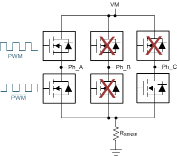
DRV8306 drv8306h-bridge-operation-normal-mode-current-limit-active.gifFigure 17. Bridge Operation in Normal Mode (Current Limit Not Active)
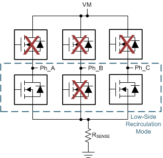
DRV8306 drv8306h-bridge-operation-normal-mode-current-limit-not-active.gifFigure 18. Bridge Operation in Current Limit Mode (Current Limit Active)
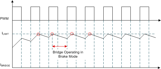
DRV8306 drv8306h-pulse-by-pulse-current-limit-operation.gifFigure 19. Pulse-by-Pulse Current-Limit Operation