ZHCSJI9A March   2019  – June 2019 BQ25886

PRODUCTION DATA.  

  1. 特性
  2. 应用
  3. 说明
    1.     简化原理图
  4. 修订历史记录
  5. Device Comparison Table
  6. Pin Configuration and Functions
    1.     Pin Functions
  7. Specifications
    1. 7.1 Absolute Maximum Ratings
    2. 7.2 ESD Ratings
    3. 7.3 Recommended Operating Conditions
    4. 7.4 Thermal Information
    5. 7.5 Electrical Characteristics
    6. 7.6 Timing Requirements
    7. 7.7 Typical Characteristics
  8. Detailed Description
    1. 8.1 Overview
    2. 8.2 Functional Block Diagram
    3. 8.3 Feature Description
      1. 8.3.1  Device Power-On-Reset
      2. 8.3.2  Device Power Up from Battery without Input Source
      3. 8.3.3  Device Power Up from Input Source
        1. 8.3.3.1 Poor Source Qualification
        2. 8.3.3.2 Input Source Type Detection
          1. 8.3.3.2.1 D+/D– Detection Sets Input Current Limit
        3. 8.3.3.3 Power Up REGN Regulator (LDO)
        4. 8.3.3.4 Converter Power Up
      4. 8.3.4  Input Current Optimizer (ICO)
      5. 8.3.5  Buck Mode Operation from Battery (OTG)
      6. 8.3.6  PowerPath Management
        1. 8.3.6.1 Narrow VDC Architecture
        2. 8.3.6.2 Dynamic Power Management
        3. 8.3.6.3 Supplement Mode
      7. 8.3.7  Battery Charging Management
        1. 8.3.7.1 Autonomous Charging Cycle
        2. 8.3.7.2 Battery Charging Profile
        3. 8.3.7.3 Charging Termination
        4. 8.3.7.4 Thermistor Qualification
          1. 8.3.7.4.1 JEITA Guideline Compliance in Charge Mode
        5. 8.3.7.5 Charging Safety Timer
      8. 8.3.8  Status Outputs
        1. 8.3.8.1 Power Good Indicator (PG)
        2. 8.3.8.2 Charging Status Indicator (STAT)
      9. 8.3.9  Input Current Limit on ILIM Pin
      10. 8.3.10 Voltage and Current Monitoring
        1. 8.3.10.1 Voltage and Current Monitoring in Boost Mode
          1. 8.3.10.1.1 Input Over-Voltage Protection
          2. 8.3.10.1.2 Input Under-Voltage Protection
          3. 8.3.10.1.3 System Over-Voltage Protection
          4. 8.3.10.1.4 System Over-Current Protection
        2. 8.3.10.2 Voltage and Current Monitoring in OTG Buck Mode
          1. 8.3.10.2.1 VBUS Over-voltage Protection
          2. 8.3.10.2.2 VBUS Over-Current Protection
      11. 8.3.11 Thermal Regulation and Thermal Shutdown
        1. 8.3.11.1 Thermal Protection in Boost Mode
        2. 8.3.11.2 Thermal Protection in OTG Buck Mode
      12. 8.3.12 Battery Protection
        1. 8.3.12.1 Battery Over-Voltage Protection (BATOVP)
    4. 8.4 Device Functional Modes
  9. Application and Implementation
    1. 9.1 Application Information
    2. 9.2 Typical Application
      1. 9.2.1 Design Requirements
      2. 9.2.2 Detailed Design Procedure
        1. 9.2.2.1 Inductor Selection
        2. 9.2.2.2 Input (VBUS / PMID) Capacitor
        3. 9.2.2.3 Output (VSYS) Capacitor
        4. 9.2.2.4 ILIM resistor
        5. 9.2.2.5 ICHGSET resistor
      3. 9.2.3 Application Curves
  10. 10Power Supply Recommendations
  11. 11Layout
    1. 11.1 Layout Guidelines
    2. 11.2 Layout Example
  12. 12器件和文档支持
    1. 12.1 器件支持
      1. 12.1.1 第三方产品免责声明
    2. 12.2 文档支持
      1. 12.2.1 相关文档
    3. 12.3 接收文档更新通知
    4. 12.4 社区资源
    5. 12.5 商标
    6. 12.6 静电放电警告
    7. 12.7 Glossary
  13. 13机械、封装和可订购信息

封装选项

机械数据 (封装 | 引脚)
散热焊盘机械数据 (封装 | 引脚)
订购信息

Typical Characteristics

CVBUS = 1µF, CPMID= 10µF, CSYS= 44µF, CBAT = 10µF, L = 1µH (DFE252012F-1R0) (unless otherwise specified)
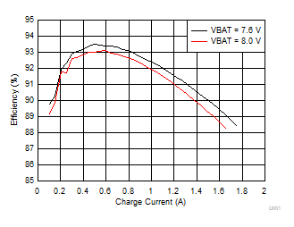
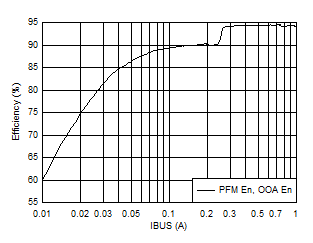
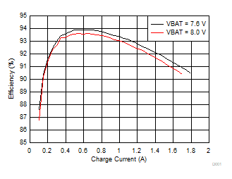
BQ25886 D001_SLUSD64_ChargeEfficiencyvsChargeCurrent.gif
VBUS = 5V
Figure 1. Charge Efficiency vs. Charge Current
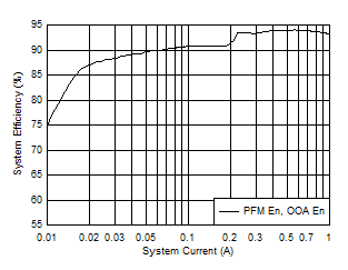
BQ25886 D016_SLUSD64_SystemEfficiencyvsSystemCurrent.gif
VBUS = 5V VBAT = 8.4V
Figure 3. System Efficiency vs. System Current
BQ25886 D018_SLUSD64_OTGEfficiencyvsVBUSOutputCurrent.gif
VBUS = 5V VBAT = 7.6V
Figure 5. OTG Efficiency vs. VBUS Output Current
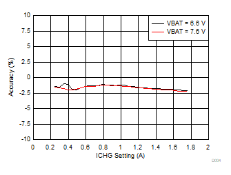
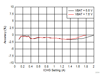
BQ25886 D004_SLUSD64_ChargeCurrentAccuracyvsICHGSetting.gif
VBUS = 5V
Figure 7. Charge Current Accuracy vs. ICHG Setting
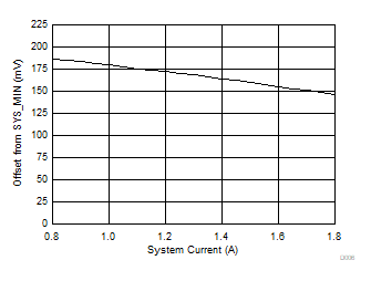
BQ25886 D006_SLUSD64_SYSMINLoadRegulation.gif
VBUS = 5V VBAT = 6V, EN_CHG = 0 SYSMIN = 7V
Figure 9. SYSMIN Load Regulation
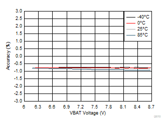
BQ25886 D010_SLUSD64_OTGVoltageRegulationvsVBATVoltage.gif
VBUS = 5.1V IBUS = 1A
Figure 11. OTG Voltage Regulation vs. VBAT Voltage
BQ25886 D001_SLUSD64_L2inductor_ChargeEfficiencyvsChargeCurrent.gif
VBUS = 5V L = 1µH (IHLP2525CZER1R0k01)
Figure 2. Charge Efficiency vs. Charge Current
BQ25886 D017_SLUSD64_L2inductor_SystemEfficiencyvsSystemCurrent.gif
VBUS = 5V VBAT = 8.4V L = 1µH (IHLP2525CZER1R0k01)
Figure 4. System Efficiency vs. System Current
BQ25886 D019_SLUSD64_L2inductor_OTGEfficiencyvsVBUSOutputCurrent.gif
VBUS = 5V VBAT = 7.6V L = 1µH (IHLP2525CZER1R0k01)
Figure 6. OTG Efficiency vs. VBUS Output Current
BQ25886 D004_SLUSD64_L2iinductor_ChargeCurrentAccuracyvsICHGSetting.gif
VBUS = 5V L = 1µH (IHLP2525CZER1R0k01)
Figure 8. Charge Current Accuracy vs. ICHG Setting
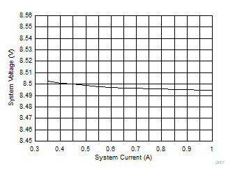
BQ25886 D007_SLUSD64_SystemLoadRegulationAfterChargeDone.gif
VBUS = 5V VBAT = 8.4V EN_CHG = 0
Figure 10. System Load Regulation After Charge Done
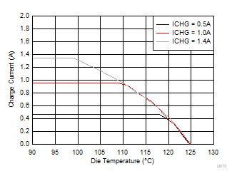
BQ25886 D015_SLUSD64_MaxCurrentTemperatureProfile.gif
VBUS = 5V VBAT = 7.6V ICHG = 0.5A, 1.0A, 1.4A
Measured on 35-µm thick copper, 4-layer board
Figure 12. Max Current Temperature Profile