ZHCS596B December 2011 – June 2019 AFE030
PRODUCTION DATA.
- 1 特性
- 2 应用
- 3 说明
- 4 修订历史记录
- 5 说明(续)
- 6 Pin Configuration and Functions
-
7 Specifications
- 7.1 Absolute Maximum Ratings
- 7.2 ESD Ratings
- 7.3 Thermal Information
- 7.4 Electrical Characteristics: Transmitter (Tx), Tx_DAC
- 7.5 Electrical Characteristics: Transmitter (Tx), Tx_PGA
- 7.6 Electrical Characteristics: Transmitter (Tx), Tx_FILTER
- 7.7 Electrical Characteristics: Power Amplifier (PA)
- 7.8 Electrical Characteristics: Receiver (Rx), Rx PGA1
- 7.9 Electrical Characteristics: Receiver (Rx), Rx Filter
- 7.10 Electrical Characteristics: Receiver (Rx), Rx PGA2
- 7.11 Electrical Characteristics: Digital
- 7.12 Electrical Characteristics: Two-Wire Interface
- 7.13 Electrical Characteristics: Zero-Crossing Detector
- 7.14 Electrical Characteristics: Internal Bias Generator
- 7.15 Electrical Characteristics: Power Supply
- 7.16 Typical Characteristics
- 8 Parameter Measurement Information
- 9 Detailed Description
- 10Application and Implementation
- 11器件和文档支持
9.3.7 ETx and ERx Blocks
The AFE030 contains a two-wire transmitter block, ETx, and a two-wire receiver block, ERx. These blocks support communications that use amplitude shift keying (ASK) with on-off keying (OOK) modulation.
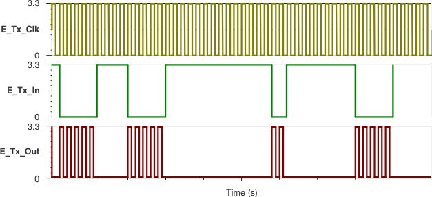
The ETx block is a gated driver that allows for transmission of a carrier input signal and modulating input signal. For typical applications, a 50-kHz square wave carrier signal is applied to E_Tx_Clk while the modulating signal is applied to E_Tx_In. The output (E_Tx_Out) is then in a high-impedance state when E_Tx_In is '1'. Figure 42 shows the relationship between E_Tx_Clk, E_Tx_In, and E_Tx_Out.
 Figure 42. ETx Block Transfer Function
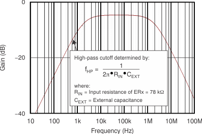
 The ERx Block consists of a low-pass analog filter configured in an inverting gain of –4.5 db. This block, along with an external capacitor, can be used to create a passband filter response as shown in Figure 43.
 Figure 43. ERx Block Frequency Response
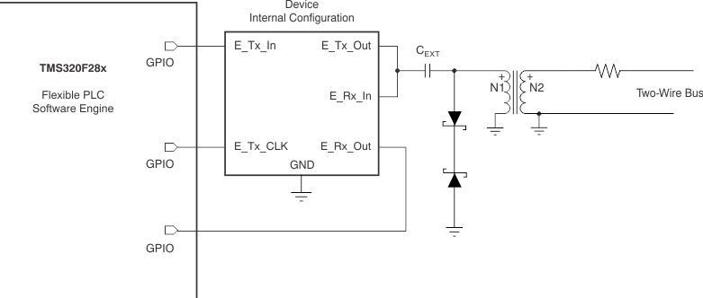
 The E_Rx_Out pin can be directly connected to either an available analog-to-digital converter (ADC) input or GPIO on the host microcontroller. Figure 44 illustrates a typical two-wire application for ETx and ERx.
 Figure 44. Typical Two-Wire Application for ETx and ERx