ZHCSCX4A June 2014 – October 2014 ADS8339
PRODUCTION DATA.
- 1 特性
- 2 应用
- 3 说明
- 4 修订历史记录
- 5 Device Family
- 6 Pin Configuration and Functions
- 7 Specifications
- 8 Parametric Measurement Information
- 9 Detailed Description
- 10Application and Implementation
- 11Power-Supply Recommendations
- 12Layout
- 13器件和文档支持
- 14机械封装和可订购信息
7 Specifications
7.1 Absolute Maximum Ratings
over operating free-air temperature range (unless otherwise noted)(1)| MIN | MAX | UNIT | ||
|---|---|---|---|---|
| +IN, –IN input | Voltage | –0.3 | +VA + 0.3 | V |
| Momentary current(2) | 130 | mA | ||
| Continuous current | ±10 | mA | ||
| +VA to GND | –0.3 | 7 | V | |
| +VBD to GND | –0.3 | 7 | V | |
| Digital input voltage to GND | –0.3 | +VBD + 0.3 | V | |
| Digital output voltage to GND | –0.3 | +VBD + 0.3 | V | |
| Temperature | Operating free-air range, TA | –40 | 85 | °C |
| Junction, TJ max | 150 | °C | ||
| VSSOP package | Power dissipation | (TJmax – TA) / θJA | °C | |
| θJA thermal impedance | 121.1 | °C/W | ||
| Maximum VSSOP reflow temperature(3) | 260 | °C | ||
(1) Stresses beyond those listed under Absolute Maximum Ratings may cause permanent damage to the device. These are stress ratings only, which do not imply functional operation of the device at these or any other conditions beyond those indicated under Recommended Operating Conditions. Exposure to absolute-maximum-rated conditions for extended periods may affect device reliability.
(2) Limit the duration for this current to less than 10 ms.
(3) The device is rated at MSL2, 260°C, as per the JSTD-020 specification.
7.2 Handling Ratings
| MIN | MAX | UNIT | |||
|---|---|---|---|---|---|
| Tstg | Storage temperature range | –65 | 150 | °C | |
| V(ESD) | Electrostatic discharge | Human body model (HBM), per ANSI/ESDA/JEDEC JS-001, all pins(1) | –1000 | 1000 | V |
| Charged device model (CDM), per JEDEC specification JESD22-C101, all pins(2) | –250 | 250 | |||
(1) JEDEC document JEP155 states that 500-V HBM allows safe manufacturing with a standard ESD control process.
(2) JEDEC document JEP157 states that 250-V CDM allows safe manufacturing with a standard ESD control process.
7.3 Recommended Operating Conditions
over operating free-air temperature range (unless otherwise noted)| MIN | NOM | MAX | UNIT | ||
|---|---|---|---|---|---|
| V+VA | Analog power-supply voltage | 4.5 | 5.0 | 5.5 | V |
| V+VBD | Digital I/O-supply voltage | 2.375 | 3.3 | 5.5 | V |
| Vref | Reference voltage | 2.25 | 4.096 | V+VA + 0.1 | V |
| f(SCLK) | SCLK frequency | 25 | MHz | ||
| TA | Operating temperature range | –40 | 85 | °C | |
7.4 Thermal Information
| THERMAL METRIC(1) | ADS8339 | UNIT | |
|---|---|---|---|
| DGS (VSSOP) | |||
| 10 PINS | |||
| RθJA | Junction-to-ambient thermal resistance | 121.1 | °C/W |
| RθJC(top) | Junction-to-case (top) thermal resistance | 29.4 | |
| RθJB | Junction-to-board thermal resistance | 32.0 | |
| ψJT | Junction-to-top characterization parameter | 0.7 | |
| ψJB | Junction-to-board characterization parameter | 31.5 | |
| RθJC(bot) | Junction-to-case (bottom) thermal resistance | N/A | |
(1) For more information about traditional and new thermal metrics, see the IC Package Thermal Metrics application report, SPRA953.
7.5 Electrical Characteristics
All minimum and maximum specifications are at TA = –40°C to 85°C, +VA = 5 V, +VBD = 5 V to 2.375 V, Vref = 4 V, and fsample = 250 kHz, unless otherwise noted. Typical specifications are at TA = 25°C.| PARAMETER | TEST CONDITIONS | MIN | TYP | MAX | UNIT | ||
|---|---|---|---|---|---|---|---|
| ANALOG INPUT | |||||||
| Full-scale input span(1) | +IN – (–IN) | 0 | Vref | V | |||
| Operating input range | +IN | –0.1 | Vref + 0.1 | V | |||
| –IN | –0.1 | 0.1 | V | ||||
| Ci | Input capacitance | 59 | pF | ||||
| Input leakage current | During acquisition | 1000 | pA | ||||
| SYSTEM PERFORMANCE | |||||||
| Resolution | 16 | Bits | |||||
| NMC | No missing codes | 16 | Bits | ||||
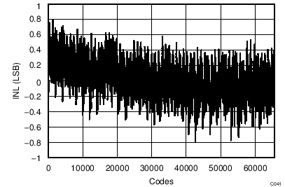
| INL | Integral linearity(7) | –2.0 | ±1.2 | 2.0 | LSB(2) | ||
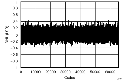
| DNL | Differential linearity | At 16-bit level | –0.99 | ±0.65 | 1.0 | LSB | |
| EO | Offset error(3) | –1.5 | ±0.3 | 1.5 | mV | ||
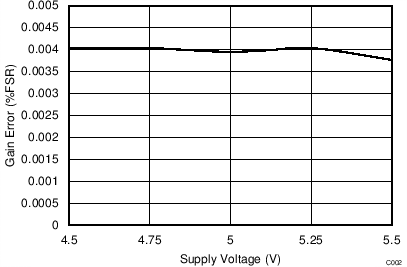
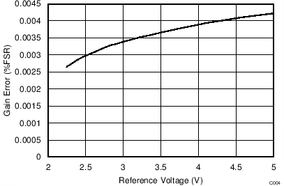
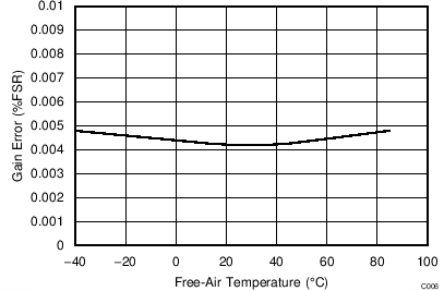
| EG | Gain error | –0.03 | ±0.0045 | 0.03 | %FSR | ||
| CMRR | Common-mode rejection ratio | With common-mode input signal = 200 mVPP
at 250 kHz |
78 | dB | |||
| PSRR | Power-supply rejection ratio | At FFF0h output code | 80 | dB | |||
| Transition noise | 0.5 | LSB | |||||
| SAMPLING DYNAMICS | |||||||
| tcnv | Conversion time | 500(4) | 3300 | ns | |||
| tacq | Acquisition time | 700 | ns | ||||
| Maximum throughput rate with or without latency |
0.25 | MHz | |||||
| Aperture delay | 2.5 | ns | |||||
| Aperture jitter, RMS | 6 | ps | |||||
| Step response | Settling to 16-bit accuracy | 600 | ns | ||||
| Overvoltage recovery | Settling to 16-bit accuracy | 600 | ns | ||||
| DYNAMIC CHARACTERISTICS | |||||||
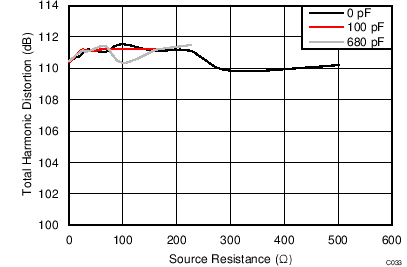
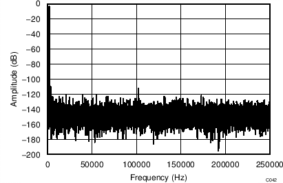
| THD | Total harmonic distortion(5) | VIN = 0.4 dB below fS at 1 kHz, Vref = 5 V | –111 | dB | |||
| VIN = 0.4 dB below fS at 10 kHz, Vref = 5 V | –106 | dB | |||||
| SNR | Signal-to-noise ratio | VIN = 0.4 dB below fS at 1 kHz, Vref = 5 V | 93.9 | dB | |||
| VIN = 0.4 dB below fS at 10 kHz, Vref = 5 V | 93.6 | dB | |||||
| SINAD | Signal-to-noise + distortion | VIN = 0.4 dB below fS at 1 kHz, Vref = 5 V | 93.8 | dB | |||
| VIN = 0.4 dB below fS at 10 kHz, Vref = 5 V | 93.4 | dB | |||||
| SFDR | Spurious-free dynamic range | VIN = 0.4 dB below fS at 1 kHz, Vref = 5 V | 113 | dB | |||
| VIN = 0.4 dB below fS at 10 kHz, Vref = 5 V | 107 | dB | |||||
| –3-dB small-signal bandwidth | 15 | MHz | |||||
| EXTERNAL REFERENCE INPUT | |||||||
| Vref | Input range | 2.25 | 4.096 | VA + 0.1 | V | ||
| Reference input current(6) | During conversion | 75 | μA | ||||
| POWER-SUPPLY REQUIREMENTS | |||||||
| Power-supply voltage | +VBD | 2.375 | 3.3 | 5.5 | V | ||
| +VA | 4.5 | 5 | 5.5 | V | |||
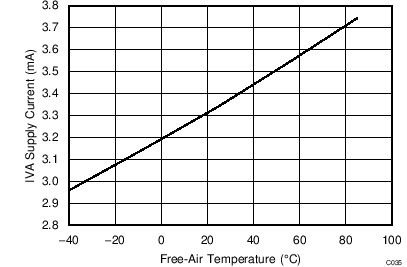
| ICC | Supply current | +VA | 250-kHz sample rate | 3.5 | 4.0 | mA | |
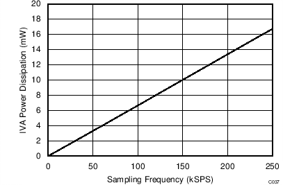
| PVA | Power dissipation | +VA = 5 V, 250-kHz sample rate | 17.5 | 20.0 | mW | ||
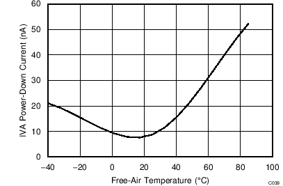
| IVApd | Device power-down current(8) | +VA = 5 V | 50 | 300 | nA | ||
| LOGIC FAMILY CMOS | |||||||
| VIH | High-level input voltage | IIH = 5 μA | 0.7 × VBD | VBD + 0.3 | V | ||
| VIL | Low-level input voltage | IIL = 5 μA | –0.3 | 0.3 × VBD | V | ||
| VOH | High-level output voltage | IOH = 2 TTL loads | VBD – 0.3 | VBD | V | ||
| VOL | Low-level output voltage | IOL = 2 TTL loads | 0 | 0.4 | V | ||
| TEMPERATURE RANGE | |||||||
| TA | Operating free-air temperature | –40 | 85 | °C | |||
(1) Ideal input span, does not include gain or offset error.
(2) LSB = least significant bit.
(3) Measured relative to actual measured reference.
(4) Refer to the CS Mode for a 3-Wire Interface section in the Device Functional Modes.
(5) Calculated on the first nine harmonics of the input frequency.
(6) Can vary by ±20%.
(7) This parameter is the endpoint INL, not best-fit INL.
(8) The device automatically enters a power-down state at the end of every conversion and remains in a power-down state as long as the device is in an acquisition phase.
7.6 Timing Requirements
All specifications are at TA = –40°C to 85°C, +VA = 5 V, and 5.5 V > +VBD ≥ 2.375 V, unless otherwise noted.| PARAMETER | TEST CONDITIONS | MIN | TYP | MAX | UNIT | |
|---|---|---|---|---|---|---|
| SAMPLING AND CONVERSION | ||||||
| tacq | Acquisition time (see Figure 47, Figure 49, Figure 50, Figure 53) |
700 | ns | |||
| tcnv | Conversion time (see Figure 47, Figure 49, Figure 50, Figure 53) |
500(1) | 3300 | ns | ||
| tcyc | Time between conversions (see Figure 47, Figure 49, Figure 50, Figure 53) |
4000 | ns | |||
| t1 | Pulse duration, CONVST high (see Figure 47, Figure 49) | 10 | ns | |||
| t6 | Pulse duration, CONVST low (see Figure 50, Figure 53, Figure 55) |
20 | ns | |||
| INPUTS AND OUTPUTS (I/O) | ||||||
| tclk | SCLK period (see Figure 47, Figure 49, Figure 50, Figure 53, Figure 55, Figure 57) | 40.0 | ns | |||
| tclkl | SCLK low time (see Figure 47, Figure 49, Figure 50, Figure 53, Figure 55, Figure 57) | 0.45 | 0.55 | tclk | ||
| tclkh | SCLK high time (see Figure 47, Figure 49, Figure 50, Figure 53, Figure 55, Figure 57) | 0.45 | 0.55 | tclk | ||
| t2 | SCLK falling edge to data remains valid (see Figure 47, Figure 49, Figure 50, Figure 53, Figure 55, Figure 57) | 5 | ns | |||
| t3 | SCLK falling edge to next data valid delay (see Figure 47, Figure 49, Figure 50, Figure 53, Figure 55, Figure 57) | 5.5 V ≥ +VBD ≥ 4.5 V | 16 | ns | ||
| 4.5 V > +VBD ≥ 2.375 V | 24 | ns | ||||
| ten | CONVST or SDI low to MSB valid (see Figure 47, Figure 50) |
5.5 V ≥ +VBD ≥ 4.5 V | 15 | ns | ||
| 4.5 V > +VBD ≥ 2.375 V | 22 | ns | ||||
| tdis | CONVST or SDI high or last SCLK falling edge to SDO 3-state (CS mode) (see Figure 47, Figure 49, Figure 50, Figure 53) |
5.5 V ≥ +VBD ≥ 4.5 V | 12 | ns | ||
| 4.5 V > +VBD ≥ 2.375 V | 15 | ns | ||||
| t4 | SDI valid setup time to CONVST rising edge (see Figure 50, Figure 53) |
5 | ns | |||
| t5 | SDI valid hold time from CONVST rising edge (see Figure 50, Figure 53) |
5 | ns | |||
| t7 | SCLK valid setup time to CONVST rising edge (see Figure 55) |
5 | ns | |||
| t8 | SCLK valid hold time from CONVST rising edge (see Figure 55) |
5 | ns | |||
(1) Refer to the CS Mode for a 3-Wire Interface subsection in the Device Functional Modes section.
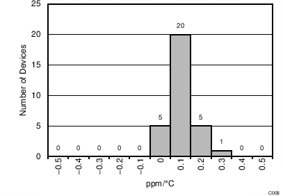
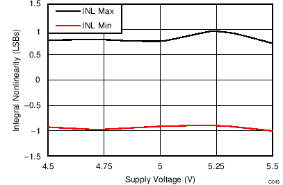
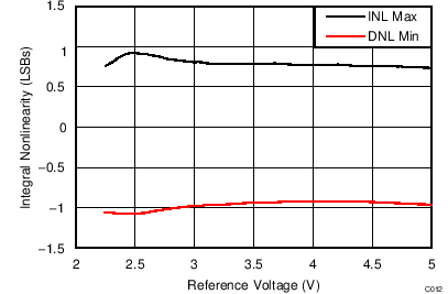
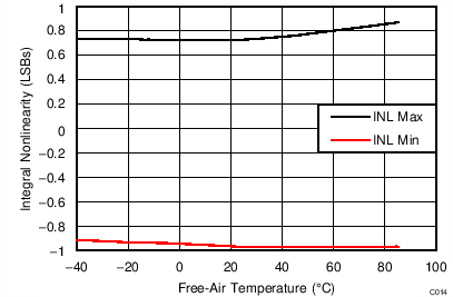
7.7 Typical Characteristics
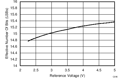
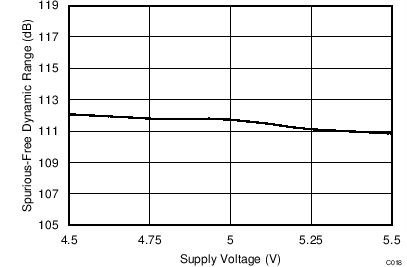
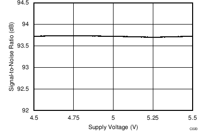
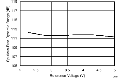
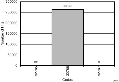
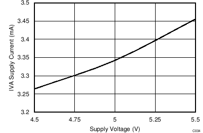
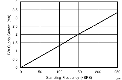
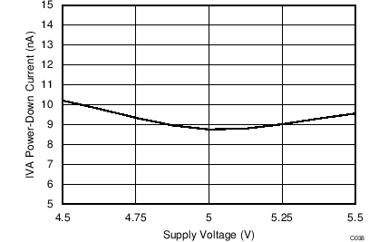
At TA = 30°C, +VA = 5 V, +VBD = 2.7 V, Vref = 4.096 V, and fsample = 250 kHz, unless otherwise noted.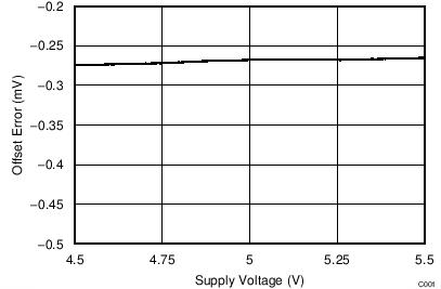
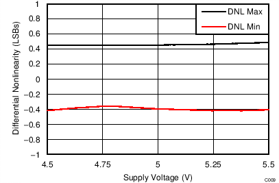
| +VBD = 2.7 V, Vref = 4.096 V, fS = 250 kSPS, TA = 30°C |
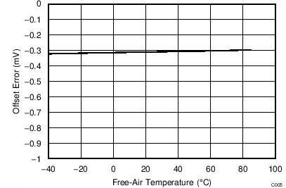
| +VBD = 2.7 V, +VA = 5 V, fS = 250 kSPS, TA = 30°C |
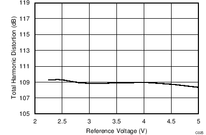
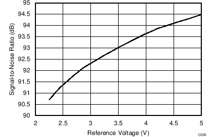
| +VBD = 2.7 V, +VA = 5 V, Vref = 5 V, fS = 250 kSPS |
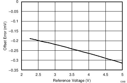
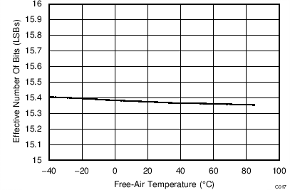
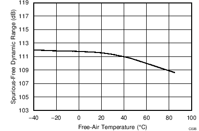
| +VBD = 2.7 V, +VA = 5 V, fS = 250 kSPS |
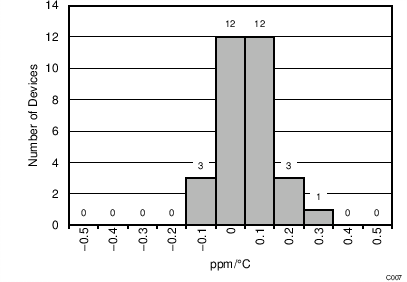
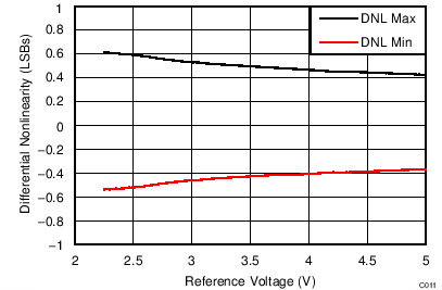
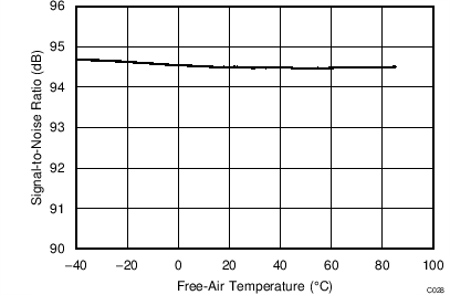
| +VBD = 2.7 V, Vref = 4.096 V, fS = 250 kSPS, TA = 30°C |
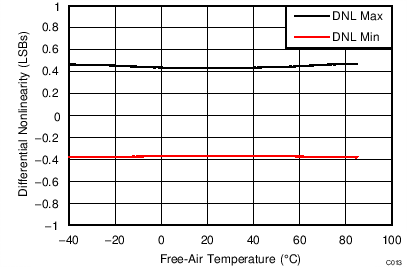
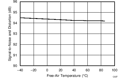
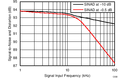
| +VBD = 2.7 V, +VA = 5 V, fS = 250 kSPS, TA = 30°C |
| +VBD = 2.7 V, +VA = 5 V, Vref = 5 V, fS = 250 kSPS |
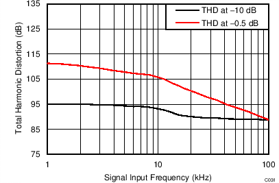
| +VBD = 2.7 V, Vref = 5 V, fIN = 1.9 kHz, fS = 250 kSPS, TA = 30°C |
| +VBD = 2.7 V, +VA = 5 V, Vref = 5 V, fIN = 1.9 kHz, fS = 250 kSPS |
| +VBD = 2.7 V, Vref = 4.096 V, fIN = 1.9 kHz, fS = 250 kSPS, TA = 30°C |
| +VBD = 2.7 V, Vref = 4.096 V, fIN = 1.9 kHz, fS = 250 kSPS, TA = 30°C |
| +VBD = 2.7 V, +VA = 5 V, fIN = 1.9 kHz, fS = 250 kSPS, TA = 30°C |
| +VBD = 2.7 V, +VA = 5 V, fIN = 1.9 kHz, fS = 250 kSPS, TA = 30°C | ||
| +VBD = 2.7 V, +VA = 5 V, Vref = 5 V, fIN = 1.9 kHz, fS = 250 kSPS |
| +VBD = 2.7 V, +VA = 5 V, Vref = 5 V, fIN = 1.9 kHz, fS = 250 kSPS |
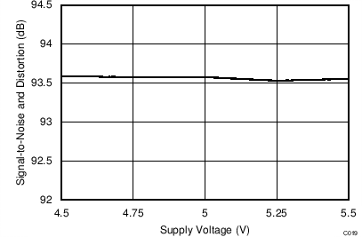
| +VBD = 2.7 V, +VA = 5 V, Vref = 5 V, fS = 250 kSPS, TA = 30°C | ||
| +VBD = 2.7 V, +VA = 5 V, Vref = 5 V, fIN = 1.9 kHz, fS = 250 kSPS, TA = 30°C |
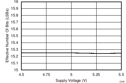
| +VBD = 2.7 V, +VA = 5 V, fS = 250 kSPS |
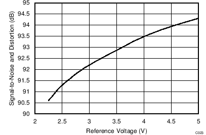
| +VBD = 2.7 V, +VA = 5 V, Vref = 5 V, TA = 30°C |
| +VBD = 2.7 V, +VA = 5 V, Vref = 4.096 V, fS = 250 kSPS |
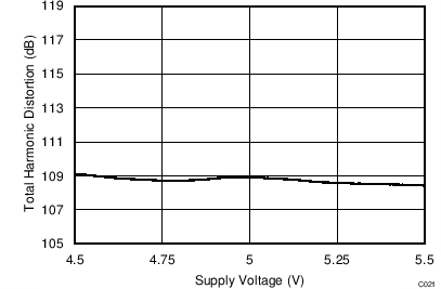
| +VBD = 2.7 V, +VA = 5 V, Vref = 5 V, fS = 250 kSPS, TA = 30°C | ||
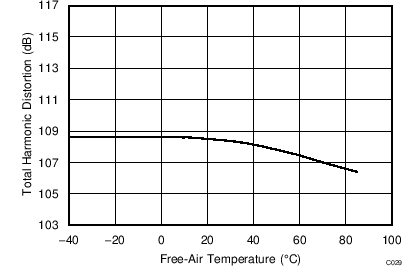
| +VBD = 2.7 V, Vref = 4.096 V, fS = 250 kSPS, TA = 30°C |
| +VBD = 2.7 V, +VA = 5 V, fS = 250 kSPS, TA = 30°C |
| +VBD = 2.7 V, +VA = 5 V, Vref = 5 V, fS = 250 kSPS |
| +VBD = 2.7 V, +VA = 5 V, Vref = 5 V, fS = 250 kSPS |
| +VBD = 2.7 V, Vref = 4.096 V, fS = 250 kSPS, TA = 30°C |
| +VBD = 2.7 V, +VA = 5 V, fS = 250 kSPS, TA = 30°C |
| +VBD = 2.7 V, +VA = 5 V, Vref = 5 V, fS = 250 kSPS |
| +VBD = 2.7 V, +VA = 5 V, fIN = 1.9 kHz, fS = 250 kSPS, TA = 30°C | ||
| +VBD = 2.7 V, Vref = 4.096 V, fIN = 1.9 kHz, fS = 250 kSPS, TA = 30°C |
| +VBD = 2.7 V, Vref = 4.096 V, fIN = 1.9 kHz, fS = 250 kSPS, TA = 30°C |
| +VBD = 2.7 V, +VA = 5 V, fIN = 1.9 kHz, fS = 250 kSPS, TA = 30°C | ||
| +VBD = 2.7 V, +VA = 5 V, fIN = 1.9 kHz, fS = 250 kSPS, TA = 30°C |
| +VBD = 2.7 V, +VA = 5 V, Vref = 5 V, fIN = 1.9 kHz, fS = 250 kSPS |
| +VBD = 2.7 V, +VA = 5 V, Vref = 5 V, fIN = 1.9 kHz, fS = 250 kSPS |
| +VBD = 2.7 V, +VA = 5 V, Vref = 5 V, fS = 250 kSPS, TA = 30°C | ||
| +VBD = 2.7 V, +VA = 5 V, Vref = 5 V, fS = 250 kSPS, TA = 30°C |
| +VBD = 2.7 V, Vref = 4.096 V, fS = 250 kSPS, TA = 30°C | ||
| +VBD = 2.7 V, +VA = 5 V, TA = 30°C |
| +VBD = 2.7 V, Vref = 4.096 V, fS = 250 kSPS, TA = 30°C |
| +VBD = 2.7 V, +VA = 5 V, Vref = 5 V, fS = 250 kSPS, TA = 30°C |
| +VBD = 2.7 V, +VA = 5 V, Vref = 5 V, fIN = 1.9 kHz, fS = 250 kSPS, TA = 30°C |