ZHCSCX4A June 2014 – October 2014 ADS8339
PRODUCTION DATA.
- 1 特性
- 2 应用
- 3 说明
- 4 修订历史记录
- 5 Device Family
- 6 Pin Configuration and Functions
- 7 Specifications
- 8 Parametric Measurement Information
- 9 Detailed Description
- 10Application and Implementation
- 11Power-Supply Recommendations
- 12Layout
- 13器件和文档支持
- 14机械封装和可订购信息
6 Pin Configuration and Functions
DGS Package
VSSOP-10
(Top View)
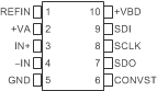
Pin Functions
| PIN | FUNCTION | DESCRIPTION | |
|---|---|---|---|
| NO. | NAME | ||
| 1 | REFIN | Input | Reference (positive) input. Decouple to GND with a 0.1-μF bypass capacitor and a 10-μF storage capacitor. |
| 2 | +VA | Supply | Analog power supply. Decouple with the GND pin. |
| 3 | +IN | Input | Noninverting analog signal input |
| 4 | –IN | Input | Inverting analog signal input. Note that this input has a limited range of ±0.1 V and is typically grounded at the input decoupling capacitor. |
| 5 | GND | Supply | Device ground. Note that this pin is a common ground pin for both the analog power supply (+VA) and digital I/O supply (+VBD). |
| 6 | CONVST | Input | Convert input. CONVST also functions as the CS input in 3-wire interface mode. Refer to the Description and Timing Diagrams sections for more details. |
| 7 | SDO | Output | Serial data output |
| 8 | SCLK | Input | Serial I/O clock input. Data (on the SDO output) are synchronized with this clock. |
| 9 | SDI | Input | Serial data input. The SDI level at the start of a conversion selects the mode of operation (such as CS or daisy-chain mode). SDI also serves as the CS input in 4-wire interface mode. Refer to the Description and Timing Diagrams sections for more details. |
| 10 | +VBD | Supply | Digital I/O power supply. Decouple with the GND pin. |