ZHCSCX4A June 2014 – October 2014 ADS8339
PRODUCTION DATA.
- 1 特性
- 2 应用
- 3 说明
- 4 修订历史记录
- 5 Device Family
- 6 Pin Configuration and Functions
- 7 Specifications
- 8 Parametric Measurement Information
- 9 Detailed Description
- 10Application and Implementation
- 11Power-Supply Recommendations
- 12Layout
- 13器件和文档支持
- 14机械封装和可订购信息
10 Application and Implementation
NOTE
Information in the following applications sections is not part of the TI component specification, and TI does not warrant its accuracy or completeness. TI’s customers are responsible for determining suitability of components for their purposes. Customers should validate and test their design implementation to confirm system functionality.
10.1 Application Information
To obtain the best performance from a high-precision successive approximation register (SAR) analog-to-digital converter (ADC), the reference driver and the input driver circuit must be optimized. This section details general principles for designing such drivers, followed by typical application circuits designed using the ADS8339.
10.1.1 ADC Reference Driver
A simplified circuit diagram for such a reference driver is shown in Figure 58.The external voltage reference must provide a low-noise, low-drift, highly-accurate voltage for the ADC reference input pin. The output broadband noise of most voltage references can be in the order of a few hundred μVRMS, which degrades the conversion result. To prevent any noticeable degradation in the noise performance of the ADC, the noise from the voltage reference must be filtered. This filtering can be done by using a low-pass filter with a cutoff frequency of a few hundred hertz.
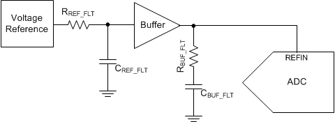 Figure 58. Reference Driver Schematic
During the conversion process, the ADS8339 switches binary-weighted capacitors onto the reference pin (REFIN). The switching frequency is proportional to the internal conversion clock frequency. The dynamic charge required by the capacitors is a function of the ADC input voltage and the reference voltage. Design the reference driver circuit such that the dynamic loading of the capacitors can be handled without degrading the noise and linearity performance of the ADC.
When the noise of the voltage reference is band-limited the next step is to design a reference buffer that can drive the dynamic load posed during the conversion cycle. The buffer must regulate the voltage at the REFIN pin of the device such that the reference voltage to the ADC stays within 1 LSB of an error at the start of each conversion. This condition necessitates the use of a large capacitor, CBUF_FLT (as shown in Figure 58). The amplifier selected as the buffer must have very low offset, temperature drift, and output impedance to drive the internal binary-weighted capacitors at the REFIN pin of the ADC without any stability issues.
10.1.1.1 Reference Driver Circuit
A more detailed circuit shows the schematic (as shown in Figure 59) of a complete reference driver circuit that generates 4.5 V dc using a single 5-V supply. This circuit can drive the reference pin of the ADS8339 at sampling rates of up to 250 kSPS. The 4.5-V reference voltage is generated using a high-precision, low-noise REF5045. The output broadband noise of the reference is further filtered using a low-pass filter with a 3-dB cutoff frequency of 16 Hz.
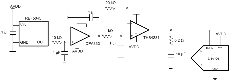 Figure 59. Reference Driver Circuit Schematic
The driver also includes a THS4281 and an OPA333. This composite architecture provides superior ac and dc performance at reduced power levels compared to a single high-performance amplifier.
The THS4281 is a high-bandwidth amplifier with very low output impedance of 1 Ω at a frequency of 1 MHz. The low output impedance makes the THS4281 a good choice for driving large capacitive loads. The high offset and drift specifications of the THS4281 are corrected using a dc-correcting amplifier (OPA333) inside the feedback loop. Thus, the composite scheme also inherits the extremely low offset and temperature drift specifications of the OPA333.
10.1.2 ADC Input Driver
The input driver circuit for a high-precision ADC mainly consists of two parts: a driving amplifier and an RC filter. An amplifier is used for signal conditioning the input voltage. The low output impedance of the amplifier functions as a buffer between the signal source and the sampling capacitor input of the ADC. The RC filter functions as an antialiasing filter that band-limits the wideband noise contributed by the front-end circuit. The RC filter also helps attenuate the sampling capacitor charge injection from the switched-capacitor input stage of the ADC. Careful design of the front-end circuit is critical to meet the linearity and noise performance of a high-precision, 16-bit ADC such as the ADS8339.
10.1.2.1 Input Amplifier Selection
Selection criteria for the input amplifier is dependent on the input signal type as well as performance goals of the data acquisition system. Some key specifications to consider when selecting an amplifier to drive the inputs of the ADS8339 are:
- Small-signal bandwidth. The small-signal bandwidth of the input amplifier must be as high as possible for a given power budget. Higher bandwidth reduces the closed-loop output impedance of the amplifier, thus allowing the amplifier to more easily drive the RC filter (with low cutoff frequency) at the inputs of the ADC. Higher bandwidth also minimizes harmonic distortion at higher input frequencies. In order to maintain overall stability, the amplifier bandwidth must satisfy Equation 1:
- Noise. Noise contribution of the front-end amplifiers must be as low as possible to prevent any degradation in the overall SNR performance of the system. As a rule of thumb, to ensure that the noise performance of the data acquisition system is not limited by the front-end circuit, keep the total noise contribution from the front-end circuit below 20% of the input-referred noise of the ADC. Noise from the input driver circuit gets band-limited by the RC filter, as given in Equation 2.
- V1 / f_AMP_PP is the peak-to-peak flicker noise in µV,
- en_RMS is the amplifier broadband noise density in nV/√Hz,
- f–3dB is the 3-dB bandwidth of the RC filter, and
- NG is the noise gain of the front-end circuit, which is equal to 1 in a buffer configuration.
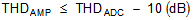
- Distortion. The ADC and the input driver introduce nonlinearity in a data acquisition block. As a rule of thumb, to ensure that the distortion performance of the data acquisition system is not limited by the front-end circuit, the distortion of the input driver must be at least 10 dB lower than the distortion of the ADC, as given in Equation 3.
- Settling Time. For dc signals with fast transients that are common in a multiplexed application, the input signal must settle to a 16-bit accuracy level at the device inputs during the acquisition time. This condition is critical in maintaining the overall linearity of the ADC. Typically, the amplifier data sheets specify the output settling performance only up to 0.1% to 0.001%, which may not be sufficient for the desired 16-bit accuracy. Therefore, the settling behavior of the input driver must always be verified by TINA™-SPICE simulations before selecting the amplifier.
where
10.1.2.2 Antialiasing Filter
Converting analog-to-digital signals requires sampling the input signal at a constant rate. Any frequency content in the input signal that is beyond half the sampling frequency is folded back into the low-frequency spectrum, which is undesirable. This process is called aliasing. An analog antialiasing filter must be used to remove the high-frequency component (beyond half the sampling frequency) from the input signal before being sampled by the ADC.
An antialiasing filter is designed as a low-pass, RC filter for which the 3-dB bandwidth is optimized based on specific application requirements. For dc signals with fast transients (including multiplexed input signals), a high-bandwidth filter is designed to allow for accurate settling of the signal at the input of the ADC. For ac signals, keep the filter bandwidth as low as possible to band-limit the noise fed into the ADC, which improves the signal-to-noise ratio (SNR) performance of the system.
The RC filter also helps absorb the sampling charge injection from the switched-capacitor input of the ADC. A filter capacitor, CFLT, is connected across the inputs of the ADC (as shown in Figure 60). This capacitor helps absorb the sampling capacitor charge injection in addition to functioning as a charge bucket to quickly charge the internal sample-and-hold capacitors during the acquisition phase.
When selecting this capacitor, as a rule of thumb, the capacitor value must be at least 10 times the ADC sampling capacitor specified on the data sheet. The input sampling capacitance is approximately 59 pF for the ADS8339. The value of CFLT must be greater than 590 pF. The capacitor must be a COG- or NPO-type because these capacitor types have a high-Q, low-temperature coefficient and stable electrical characteristics under varying voltages, frequency, and time.
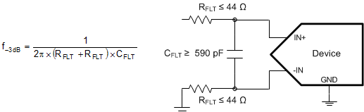 Figure 60. Antialiasing Filter
NOTE
Driving capacitive loads can degrade the phase margin of the input amplifiers, thus making the amplifier marginally unstable. To avoid stability issues, series isolation resistors (RFLT) are used at the output of the amplifiers. A higher value of RFLT is helpful from the amplifier stability perspective. Distortion increases with source impedance, input signal frequency, and input signal amplitude. The selection of RFLT thus requires a balance between stability and distortion of the design.
TI recommends limiting the value of RFLT to a maximum of 44 Ω in order to avoid any significant degradation in linearity performance for the ADS8339. The tolerance of resistors can be 1% because the differential capacitor at the input balances the effects resulting from resistor mismatch.
The input amplifier bandwidth must be much higher than the cutoff frequency of the antialiasing filter. TI strongly recommends running a SPICE simulation to confirm that the amplifier has more than 40° phase margin with the filter that is designed. Simulation is critical because some amplifiers may require more bandwidth than others to drive similar filters. If an amplifier has less than 40° phase margin with 44-Ω resistors, using a different amplifier with higher bandwidth or reducing the filter cutoff frequency with a larger differential capacitor is advisable.
10.2 Typical Application
This section describes a typical application circuit using the ADS8339. The circuit is optimized to derive the best ac performance. For simplicity, power-supply decoupling capacitors are not shown in these circuit diagrams.
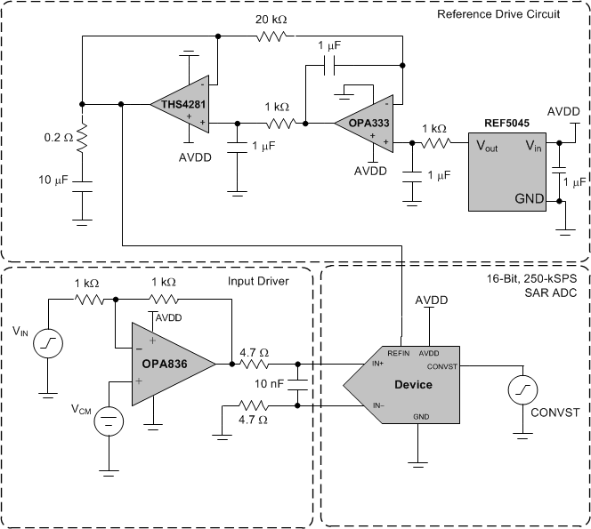 Figure 61. Single-Ended Input DAQ Circuit for Lowest Distortion and Noise at 250 kSPS
10.2.1 Design Requirements
The application circuit for the ADS8339 (as shown in Figure 61) is optimized for lowest distortion and noise for a 10-kHz input signal to achieve:
- –106-dB THD and 93-dB SNR at a maximum specified throughput of 250 kSPS.
10.2.2 Detailed Design Procedure
In the application circuit, the input signal is processed through a high-bandwidth, low-distortion, inverting amplifier and a low-pass RC filter before being fed to the ADC.
The reference driver circuit illustrated in Figure 59 generates 4.5 V dc using a single 5-V supply. This circuit is suitable to drive the reference at sampling rates of up to 250 kSPS. To keep the noise low, a high-precision REF5045 is used. The output broadband noise of the reference is heavily filtered by a low-pass filter with a 3-dB cutoff frequency of 16 Hz.
The reference buffer is designed in a composite architecture to achieve superior dc and ac performance at reduced power consumption. The low output impedance makes the THS4281 a good choice for driving large capacitive loads that regulate the voltage at the reference input pin of the ADC. The high offset and drift specifications of the THS4281 are corrected by using a dc-correcting amplifier (such as the OPA333) inside the feedback loop.
For the input driver, as a rule of thumb, the distortion of the amplifier must be at least 10 dB less than the ADC distortion. The distortion resulting from variation in the common-mode signal is eliminated by using the driver in an inverting gain configuration. This configuration also eliminates the need for an amplifier that supports rail-to-rail input. The OPA836 is a good choice for an input driver because of its low-power consumption and exceptional ac performance (such as low distortion and high bandwidth).
Finally, the components of the antialiasing filter are chosen such that the noise from the front-end circuit is kept low without adding distortion to the input signal.
10.2.3 Application Curve
To ensure that the circuit meets the design requirements, the dc noise performance and the frequency content of the digitized output is verified. The input is set to a fixed dc value at half the reference. The histogram of the output code shows a peak-to-peak noise distribution of four codes which translates to 14 bits of noise-free bits.
An ac signal at 10 kHz is then fed to the input. The FFT of the output shows a THD of –106 dB and an SNR of 92 dB, which is close to the design requirements.
| VDIFF = Vref / 2, 2048 data points, standard deviation = 0.41 bits |
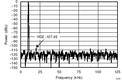
| SNR = 92 dB, THD = – 106 dB, number of samples = 1024 |
10.3 Do's and Don'ts
- Use multiple capacitors to decouple the dynamic current transients at various input pins including the reference, supply, and input signal.
- Parasitic inductance can induce ringing on the clock signal. Include a resistor on the SCLK pin to clean up the clock edges.